Turnkey electronic assemblies optimized for thermal stability, high current density, and harsh operating conditions.



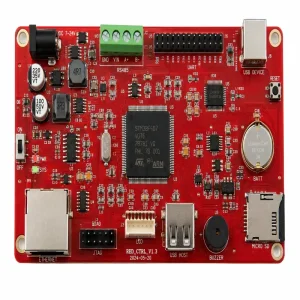
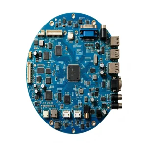
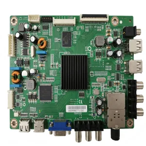
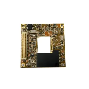
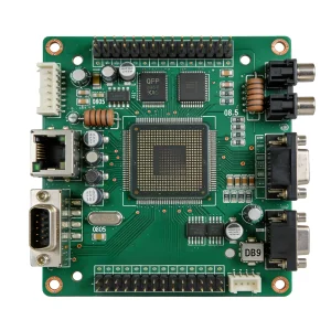
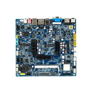
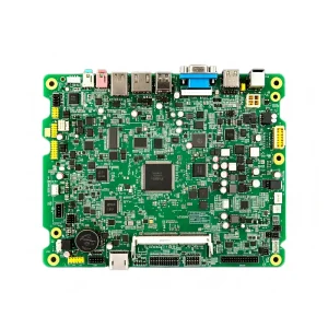
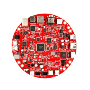
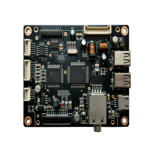
Modern electronic products increasingly hinge on the stability and processing bandwidth of the central motherboard or main PCB assembly.
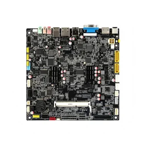
As computational loads shift from centralized cloud servers to edge-computing hardware, the standard main PCB board has evolved from a basic point-to-point interconnect layout into an ultra-dense platform. Any-layer HDI, microvias with copper filling, and controlled-impedance differential lines are vital to handling gigahertz-range signaling without electromagnetic distortion.
Next-generation automotive TCU assemblies, multi-kilowatt solar inverters, and heavy-duty electric tools generate localized heat spikes. Engineering successful motherboards necessitates advanced substrate materials such as high-Tg FR-4, ceramic cores, thick copper (>3oz), and strategic aluminum backplanes to avoid thermal throttling and delamination.
Global OEMs can no longer treat procurement as transactional. ISO 13485 for medical automation and IATF 16949 for automotive drivetrains impose absolute traceability. Solder joint integrity, voiding rates under Ball Grid Arrays (BGA), and ionic contamination limits demand continuous automated in-line inspection and process telemetry.
The convergence of localized parts fabrication, active distributor channels, and high-velocity engineering reduces development cycles from months to days.
Situated within the Greater Bay Area electronics nexus, Shenzhen facilities access vast authorized component hubs. Over 100 franchise distribution lines (including Arrow, Mouser, Avnet, Microchip, and STMicroelectronics) provide physical delivery within hours, eliminating international transit latency and stabilizing line availability against sudden global chip allocation shifts.
Western contract manufacturers typically require prohibitively large order minimums to justify surface mount tooling and feeder programming. Chinese intelligent manufacturing hubs operate on dynamic, quick-setup architectures. Prototype verification lots are converted to automated mass runs seamlessly, enabling overseas design houses to validate complex hardware without committing capital to excessive inventory.
Direct production capability metrics maintained across high-speed Yamaha and Panasonic automated lines.
| Process Parameter | Advanced Capability (Prototype & Small Batch) | High-Volume Manufacturing (Standard Mass Production) | Inspection & Verification Protocol |
|---|---|---|---|
| Layer Count Range | 1 to 32 Layers (Blind/Buried Via Architecture) | 1 to 16 Layers (Rigid, Rigid-Flex, Metal-Core) | AOI, Microsection Analysis, TDR Impedance Test |
| SMT Component Placement | 01005 (0402 Metric), Micro-BGA 0.3mm Pitch | 0201, 0402, Standard QFP/BGA, Odd-form DIP | Inline 3D-SPI (Solder Paste) & 3D-AOI Optical Scan |
| Substrate Selection | Rogers, Megtron 6, Isola, Polyimide, Aluminum | High-Tg FR-4 (TG170-180), Standard FR-4, CEM-3 | IPC-TM-650 Thermal Stress & Flammability UL94-V0 |
| BGA Solder Void Rate | < 8% (Aerospace & Automotive Class 3) | < 15% (IPC-A-610 Class 2 Standard) | High-Resolution 2D/3D X-Ray Inspection (AXI) |
| Surface Finishing | ENIG, ENEPIG, Immersion Tin, Hard Gold Plating | Lead-Free HASL, Standard ENIG, OSP | XRF Plating Thickness Analyzer & Solderability Testing |
| End-of-Line Reliability | Custom Functional Test (FCT), IC In-System Burn-in | Bed-of-Nails ICT, Automated High-Voltage Hi-Pot | Custom Test Fixtures, Automated Firmware Checksum |
How our mainboard architectures are deployed across high-demand mission-critical environments.
Main control motherboards for automotive TCUs and Electronic Power Steering (EPS) operate in harsh mechanical environments. Assemblies require IATF 16949-grade process validation, heavy conformal coating (polyurethane or silicone) to prevent moisture corrosion, and thick copper layers engineered to handle high current pulses without delamination.
Solar inverters and DIN Rail industrial switching supplies utilize double-sided SMT boards integrated with heavy through-hole inductive filtering. The design balances microcontrollers running high-speed PWM algorithms with galvanic isolation zones compliant with IEC 62109 creepage and clearance safety distances.
Modern Optical Network Units (ONU) and VoIP enterprise systems feature gigabit-speed Ethernet routing and high-frequency RF transmission traces. Controlled impedance matching (±5%), low-loss dielectric laminates, and zero-crosstalk trace isolation ensure clean packet transmission without packet drop or excessive jitter.
Evaluating the shift in enterprise electronics manufacturing requirements from transactional quoting to strategic integration.
Global procurement teams reject vendors that simply place parts blindly. Modern buyers require upfront Design for Manufacturability (DFM) and Design for Assembly (DFA) audits. Identifying insufficient solder clearances, thermal shadowing, and unbalanced copper pours before stencils are cut preserves capital and protects development schedules.
Supply chain security requires component provenance. Enterprise manufacturing execution systems (MES) bind barcode records to individual main PCB serial numbers, registering the precise solder reel lot, reflow thermal profile curve, and test vector results for every finished product leaving the facility.
Supply disruption has driven buyers toward turnkey electronic manufacturing solutions. Instead of managing dozens of component suppliers, procurement managers rely on an integrated EMS partner with engineering teams capable of suggesting pin-compatible drop-in replacements for obsolete or inflated components without sacrificing certification integrity.
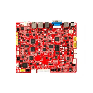
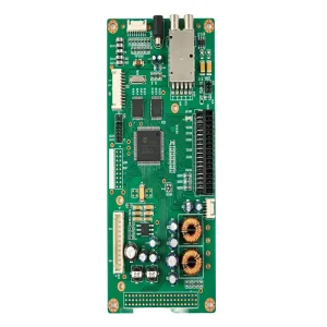
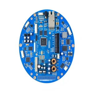
Robust electronics manufacturing service solutions across medical diagnostics, avionics, enterprise lighting, and automation.
Clear, unhedged answers to questions on quality systems, lead times, fabrication limits, and supply chain controls.
