
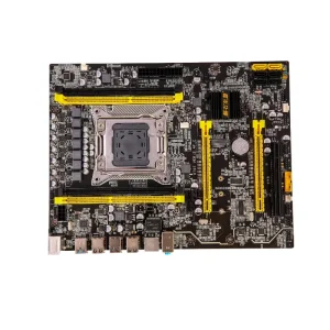
Explore high-complexity manufacturing deliverables validated for healthcare diagnostics, IoT communication, renewable power, and sensor integration.
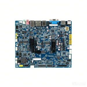
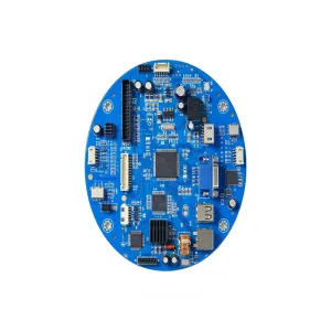
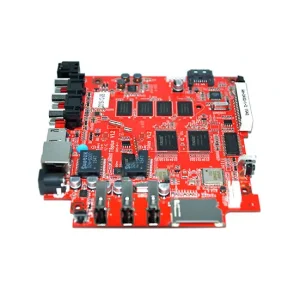
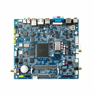
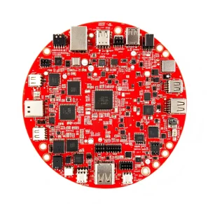
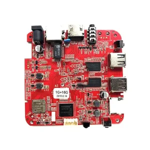
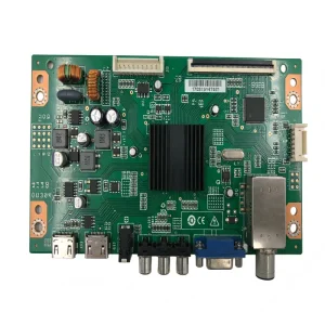
A technical overview of modern electronic manufacturing service (EMS) dynamics across North America, Europe, and Asia-Pacific.
Modern electronic engineering requires rapid transitions from NPI (New Product Introduction) to full-scale fabrication. Global procurement strategies require agile fabrication facilities capable of processing multi-layer High-Density Interconnect (HDI) and flex-rigid architectures with minimal turnaround friction.
With edge computing, sub-6 GHz RF, and high-speed data interconnects dominating current hardware topologies, the demand for controlled impedance, low-loss dielectric substrates (such as Rogers and high-Tg FR-4), and micro-via laser drilling has grown exponentially.
The convergence of consumer IoT into medical diagnostic and automotive domains mandates compliance protocols including RoHS, REACH, UL94V-0 flammability ratings, and IPC-A-610 Class 2/3 manufacturing standards across every physical production lot.
How localized clustering and intelligent digital procurement mitigate component shortages and optimize build cycles.
Situated in Bao'an, Shenzhen, our facility operates at the nexus of the world's dense electronic ecosystem. Sourcing passive components, specialty substrates, custom tooling, and metal stampings occurs within a verified 20-kilometer radius, drastically reducing standard transit times.
STHL partners with certified global distributors and authorized brand manufacturers (including Digi-Key, Mouser, Arrow, and direct IC foundries). Our centralized ERP tracks lot codes, shelf lives, and moisture sensitivity levels (MSL) with complete traceability.
We eliminate the traditional barrier between small-batch prototype validation and high-volume mass manufacturing. Running 7 high-speed SMT lines and 2 automated DIP/THT lines allows smooth scaling without tooling discrepancies or requalification delays.
In-depth technical breakdown of customized Make PCB assemblies engineered for specialized industrial demands.
Substrates designed for magnetic resonance imaging (MRI) and smart blood glucose monitoring systems mandate ultra-low electrical noise, non-magnetic materials, and high-frequency RF integrity. Our production applies controlled differential impedance alongside rigorous X-ray inspection on fine-pitch BGAs.
DC-DC power converters, motor controllers, and automotive inverters necessitate heavy-copper PCB designs (3oz to 6oz) to dissipate thermal energy efficiently. Wave-soldered THT components are tested via automated optical inspection (AOI) to eliminate structural micro-fractures under high vibration.
Explosion-proof enclosures and emergency environmental monitoring arrays demand high surface insulation resistance (SIR). We utilize robotic conformal coating (silicone, acrylic, and polyurethane) to shield critical traces from volatile organic vapors, salt spray, and extreme humidity.
Verified operational parameters and engineering tolerance standards deployed on STHL manufacturing lines.
| Process Category | Technical Capability & Parameter Tolerances |
|---|---|
| Layer Count & Substrates | 1 to 32 Layers; FR-4 (Normal, Mid, High-Tg), Rogers, PTFE, Polyimide (Flex), Rigid-Flex, Aluminum Core, Copper Substrates, Ceramic. |
| Surface Finishes | Lead-Free HASL, ENIG (Electroless Nickel Immersion Gold), ENEPIG, Immersion Silver, Immersion Tin, OSP, Hard Gold Plating. |
| SMT Component Placement | 01005 (imperial), 0201, 0402, QFN, BGA, micro-BGA (0.35mm ball pitch), POP (Package on Package), fine-pitch connectors. |
| Minimum Trace & Spacing | Inner layers: 2.5 mil / 2.5 mil (0.065mm); Outer layers: 3 mil / 3 mil (0.075mm); Controlled impedance tolerance: ±5% to ±10%. |
| Hole Technology | Laser micro-vias (0.075mm), mechanical mechanical blind/buried vias, via-in-pad plated over (VIPPO), resin-filled holes. |
| Quality & Test Protocols | 3D Solder Paste Inspection (SPI), Online 3D AOI, High-Resolution 2D/3D X-Ray, In-Circuit Testing (ICT), Flying Probe, Custom FCT Racks. |
| System Certifications | IATF 16949 (Automotive), ISO 13485 (Medical), ISO 9001:2015, ISO 14001:2015, IPC-A-610 Class 2/3 certified workmanship. |
Robust institutional mechanisms designed to safeguard international intellectual property and support seamless customs logistics.
Prior to reviewing Gerber archives, schematics, or firmware, STHL executes legally binding bilateral NDAs. File access is segmented via encrypted internal servers, ensuring that your proprietary IP remains accessible solely to designated project engineers.
Every PCBA unit is marked with a 2D DataMatrix code tracking solder paste temperature profiles, reel lot numbers, reflow oven zone curves, and functional test data points. This provides complete audit trails required by medical and automotive clients.
Navigating global tariff policies and customs declarations is managed end-to-end. We provide complete documentation including Certificates of Conformance (CoC), material declarations, MSDS, and automated export clearances across more than 90 destination nations.
Direct technical answers addressing fabrication lead times, file submissions, testing parameters, and volume scaling.
Precision-assembled electronics designed for smart security, wireless communications, healthcare, and telecommunications.
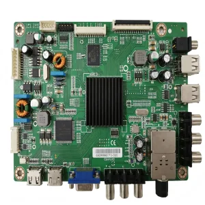
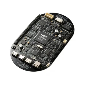
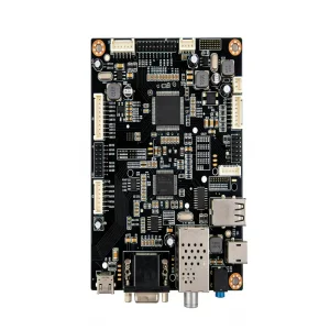
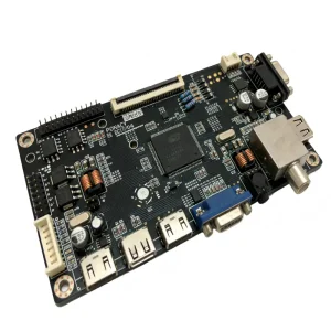
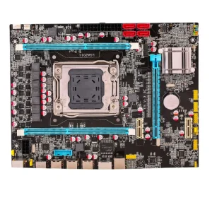
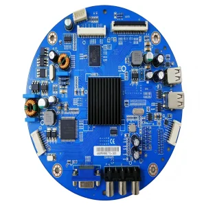
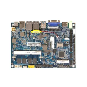
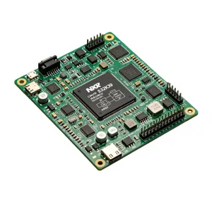
Send your Gerber files and BOM for an immediate DFM report and comprehensive pricing from our senior engineering team.
Request Free Engineering DFM & Quote