Enterprise Engineering & Sourcing Guide

High-Quality Multi Layer PCB Service & Factories

Precision multi-layer interconnection, microvia HDI engineering, and turnkey PCBA assembly delivering IPC Class 3 structural integrity for high-reliability global electronics.

Production Portfolio

Precision Multi-Layer PCB Assembly Implementations

Explore production-grade high-layer and high-density assemblies deployed across automotive telemetry, industrial edge nodes, and critical instrumentation.
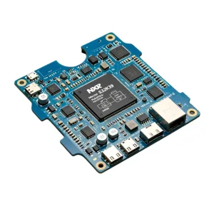
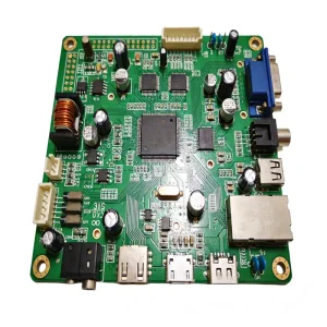
High-Quality Anesthesia Machine PCB Assembly
High-Quality Anesthesia Machine PCB Assembly--STHL Manufacturer, Manufacturers
Inspect Technical Details
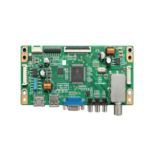
OEM Edge-Lit LED Backlight PCB Assembly
OEM Edge-Lit LED Backlight PCB Assembly--STHL Factories, Factory
Inspect Technical Details
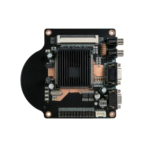
High-Quality Heads-Up Display HUD PCBA Assembly
High-Quality Heads-Up Display (HUD) PCBA Assembly--STHL Manufacturer, Factories
Inspect Technical Details
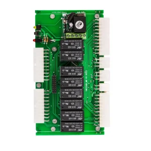
High-Quality Alarm System PCB Assembly
High-Quality Alarm System PCB Assembly--STHL Factories, Factory
Inspect Technical Details
OEM High Quality Automotive PCBA Factory
OEM High Quality Automotive PCBA Factory PCB Housing Service Double Side PCBA Factories, Factory
Inspect Technical Details
China Soil Detector PCB Assembly
China Soil Detector PCB Assembly Manufacturers, Factory
Inspect Technical Details
OEM Head-Up Display HUD PCB Assembly
OEM Head-Up Display (HUD) PCB Assembly Manufacturers, Factory
Inspect Technical Details
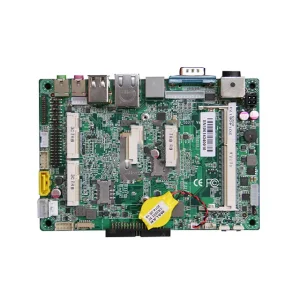
OEM Home Automation Controllers PCBA
OEM Home Automation Controllers PCBA Assembly--STHL Manufacturer, Factories
Inspect Technical Details
Enterprise Procurement Analysis

Macro Dynamics Driving High-Layer Interconnect Demand

Strategic hardware engineering teams balance layer stack-up density, dielectric losses, and cross-talk suppression against total landing costs and time-to-market constraints.

20+
Years EMS Expertise
10,000+
Square Meter Facility
99.5%
On-Time Logistics Rate
50+
In-House Engineers

Controlled Impedance & SI

As switching frequencies exceed multi-gigahertz thresholds in 5G and radar architectures, multi-layer stack-up designs must maintain tightly managed dielectric tolerances (±5% to ±10%) across stripline and microstrip geometries to eliminate reflections and eye-diagram degradation.

Thermal Dissipation Routing

High-density packaging generates excessive thermal flux densities. Modern multi-layer fabrication integrates embedded copper coins, thermally conductive prepregs, and dense arrays of thermal microvias to transfer heat away from power ICs directly into chassis heat sinks.

Mitigation of Supply Chain Risk

Procuring multi-layer boards demands end-to-end BOM resilience. Our 100+ vetted supply relationships guarantee lifecycle traceability, rapid alternate qualification for long-lead passives, and active countermeasure testing against grey-market counterfeit components.

Engineering Specifications

Advanced Multi-Layer PCB Capabilities & Stack-Up Matrix

STHL maintains full technological capability from quick-turn prototyping to high-volume multi-layer builds, strictly adhering to IPC-A-610 Class 2 and Class 3 manufacturing criteria.

Process Parameter Standard Capability Advanced / HDI Capability
Layer Count 2 – 32 Layers Up to 64 Layers (Rigid / Rigid-Flex)
Minimum Trace Width / Spacing 3 / 3 mil (0.075 / 0.075 mm) 2 / 2 mil (0.05 / 0.05 mm) ultra-fine pitch
Microvia / Laser Drill Technology Mechanical Drill: 0.15 mm Laser Via: 0.075 mm (Any-Layer HDI 1+N+1 to 4+N+4)
Core Dielectrics Supported Standard FR-4, Mid/High-Tg (Tg 170°C+) Rogers, Megtron 6, Shengyi, Halogen-Free, Ceramic, Aluminum
Aspect Ratio 8:1 Through-Hole 12:1 High-Reliability Plated Through-Hole
Surface Finishes HASL, Lead-Free HASL, ENIG ENEPIG, Immersion Silver, Immersion Tin, Hard Gold Plating
Quality Assurance Audits 100% AOI, Flying Probe, Fixture E-Test 3D X-Ray (AXI), Microsection Cross-Sectioning, TDR Impedance Test
Industry Solutions

Mission-Critical Sector Integration

Multi-layer printed circuit boards serve as the backbone for sophisticated compute, power transmission, and medical monitoring systems across global operating environments.

Automotive Systems

Certified under IATF 16949, our assemblies power head-up displays (HUD), ADAS compute units, and battery management nodes exposed to extreme thermal cycling.

Medical Diagnostics

ISO 13485 compliance guarantees traceability and low-voiding solder joints across anesthesia machines, patient telemetry, and complex CT scan control planes.

Industrial Edge & IoT

From environmental sensors and smart soil detectors to industrial PLCs, multi-layer designs provide ruggedized noise immunity and stable field operation.

Communications & IT

Dense RF routing, backplane boards, enterprise modems, and optical transceiver modules requiring sub-micron component placement and controlled impedance matching.

Trust & Governance

Global Compliance, IP Security & Engineering Support

Mitigate international offshore procurement friction through comprehensive institutional certifications, non-disclosure execution, and dedicated DFM engineering reviews.

Strict IP Protection

We execute legally binding bilateral NDAs prior to RFQ examination. Firmware, proprietary stack-up coordinates, and schematics are segmented within secure MES networks accessible only to authorized engineers.

Multi-Standard Certified

Operations are independently audited and certified under IATF 16949 (Automotive), ISO 13485 (Medical), ISO 9001 (Quality Management), and ISO 14001 (Environmental), ensuring uniform compliance across jurisdictions.

Global Seamless Logistics

Exporting to more than 90 countries with direct customs clearances, localized account management across North America and Europe, and specialized packaging safeguarding bare and assembled multi-layer boards.

Procurement Knowledge Base

Frequently Asked Questions on Multi-Layer PCB Assembly

In-depth responses covering engineering verification, minimum batch requirements, high-frequency design choices, and factory test methodologies.

What factors govern the selection of core dielectrics in high-layer count boards?
Core dielectric selection depends directly on operating frequency, thermal load, and maximum allowable signal loss (Df). While standard FR-4 (Tg 130-140°C) is cost-effective for low-speed digital routing, high-layer multi-layer stack-ups utilize High-Tg FR-4 (Tg 170°C+) to resist z-axis expansion during reflow. For high-speed digital and RF links above 10 Gbps, low-loss laminate families such as Rogers RO4350B or Megtron 6 are integrated as hybrid stack-ups to balance signal integrity against fabrication costs.
How does STHL verify through-hole plating integrity across 16+ layer boards?
High aspect ratio plated through-holes (PTH) present risk of barrel cracking or thin knee plating. Our manufacturing facilities employ continuous pulse plating cells and periodic metallurgical microsection audits. Boards undergo thermal stress conditioning followed by cross-sectional microscopy to verify copper thickness inside hole walls meets or exceeds IPC Class 3 standards (average 25µm / 1 mil), accompanied by automated four-wire Kelvin resistance measurements.
What is the minimum order quantity (MOQ) for custom multi-layer fabrication and SMT?
STHL enforces no minimum order quantity (No MOQ). We handle engineering verification prototypes (EVT), design verification testing (DVT) batches from 1 to 50 units, and seamless production line transfer into continuous high-volume mass manufacturing across our 7 automated SMT lines.
How are buried, blind, and microvias inspected after full assembly?
Inner-layer laser microvias and filled vias (VIPPO) are first evaluated during PCB fabrication using automated optical inspection (AOI) and electrical net-list testing. Once SMT components like fine-pitch BGAs, QFNs, and CSPs are assembled, high-resolution 3D Automated X-ray Inspection (AXI) is deployed to inspect solder void percentages, bridging, and wetting reliability hidden underneath physical packages.
What files and data packages are required to initiate an engineering DFM audit?
To conduct a complete Design for Manufacturability (DFM) and Design for Assembly (DFA) review, our engineering team requires RS-274X Gerber or ODB++ fabrication files, layer stack-up definitions, IPC-D-356 netlists, Bill of Materials (BOM) including exact manufacturer part numbers (MPNs), pick-and-place centroid files, and clear testing protocols. Feedback is returned within 24 business hours.
Expanded Production Range

High-Layer Industrial, IoT & Communication Assemblies

Explore additional mission-critical PCBA modules designed for long-lifecycle reliability in networked enterprise and field monitoring deployments.
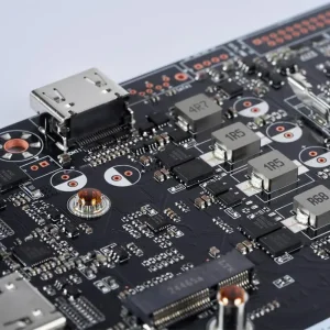
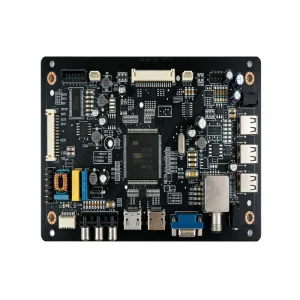
OEM LED Matrix Board PCB Assembly
OEM LED Matrix Board PCB Assembly--STHL Manufacturer, Service
Inspect Technical Details
OEM Modem PCB Assembly
OEM Modem PCB Assembly--STHL Manufacturer, Manufacturers
Inspect Technical Details
High-Quality Communication PCBA Application
High-Quality Communication PCBA Application: Connecting the World with Precision Manufacturers, Factory
Inspect Technical Details
China Wireless Network Router PCB Assembly
China Wireless Network Router PCB Assembly--STHL Service, Factory
Inspect Technical Details
High-Quality Voice Assistant Device PCBA Assembly
High-Quality Voice Assistant Device PCBA Assembly--STHL Manufacturer, Manufacturers
Inspect Technical Details
OEM Wireless Phone PCB Assembly
OEM Wireless Phone PCB Assembly--STHL Manufacturer, Manufacturers
Inspect Technical Details
High-Quality Indoor Security Camera PCBA
High-Quality Indoor Security Camera PCBA Assembly--STHL Manufacturer, Service
Inspect Technical Details
China CT Scanner PCB Assembly
China CT Scanner PCB Assembly--STHL Manufacturer, Manufacturers
Inspect Technical Details