
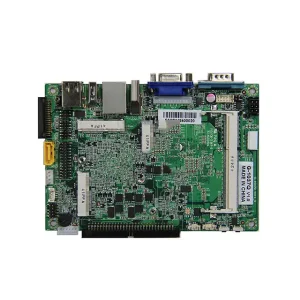
Engineered with zero-defect methodologies, comprehensive SMT/THT integration, and automated optical and multi-axis X-ray validation.
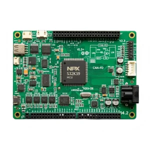
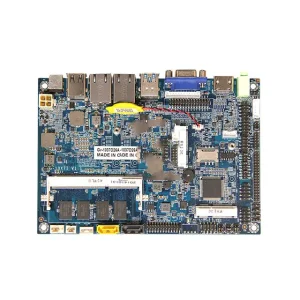
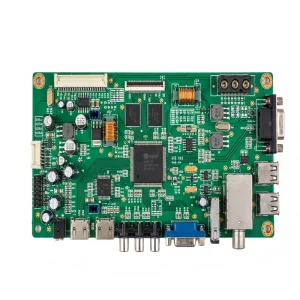
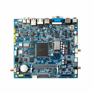
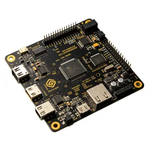
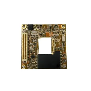
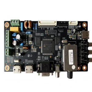
Analyzing how tier-1 OEMs and hardware unicorns de-risk their electronic manufacturing pipelines across dynamic geopolitical and supply constraints.
Modern global procurement strategies mandate real-time BOM health scoring. Sourcing teams prioritize PCBA manufacturers with authenticated component access (Digi-Key, Mouser, Avnet, Arrow, STMicroelectronics) and algorithmic alternate part crossing for MLCCs, MOSFETs, and MCUs.
Engineering departments require proactive Design for Manufacturing (DFM) and Design for Assembly (DFA) audits before bare-board fabrication. Discovering aspect ratio issues, copper-to-edge balance defects, or component tombstoning hazards upstream prevents expensive production delays.
For medical diagnostics (ISO 13485) and automotive modules (IATF 16949), full traceability down to the specific reflow oven thermal profile, solder paste batch, pick-and-place nozzle log, and X-ray voiding percentage is an unconditional contractual barrier.
How high-precision automated systems transform bare boards and raw microcomponents into mission-critical hardware assemblies.
Utilizing high-precision electro-polished laser stencils, nanometer-level alignment cameras deposit SAC305 or SnBiAg alloy pastes. Subsequent 3D Solder Paste Inspection (SPI) guarantees volumetric precision, eliminating 70% of potential surface mount defects before thermal cycling.
Yamaha and Panasonic multi-gantry mounters deliver placement precision up to ±15 microns at 0.035s per part. From miniature 01005 passive passives to ultra-fine pitch Ball Grid Arrays (BGA, micro-BGA) and Quad-Flat No-Leads (QFN), placement accuracy is monitored by smart vision sensors.
10-zone nitrogen (N2) forced convection reflow ovens maintain tight delta-T profiles to avert pad oxidation and thermal stress. Dual-wave and selective wave soldering lines process Through-Hole Technology (THT/DIP) components without damaging adjacent high-density SMT layers.
Automated Optical Inspection analyzes solder filleting, tombstoning, and component polarity across multiple lighting spectrums. For concealed BGA, CSP, and QFN solder balls, 3D computed tomography X-Ray (AXI) measures solder voiding rates to keep them well below the strict IPC 15% ceiling.
Robotic atomized spray and selective film coaters apply acrylic, polyurethane, or silicone coatings. Critical against moisture ingress, salt spray corrosion, thermal shocks, and vibration in challenging aerospace, EV charger, and industrial petrochemical monitoring deployments.
Custom bed-of-nails test fixtures and flying probes assess continuity, shorts, and passive values. Microcontroller flashing, boundary scan, and full-load functional testing under simulated field conditions ensure every outgoing board works right out of the carton.
Anticipating structural engineering shifts towards high-density interconnection, wide-bandgap semiconductors, and sustainable circular manufacturing.
Scalable electronic manufacturing services spanning low-power wearable modules up to automotive-grade high-voltage conversion systems.

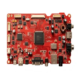
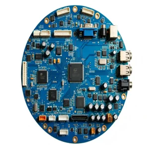

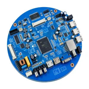

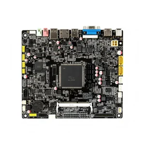
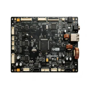
How international hardware enterprises align with stringent regional certifications across North American, European, and Asian supply chains.
STHL provides strict compliance documentation adhering to UL 94V-0 flammability ratings, FCC Part 15 Class B electromagnetic interference rules, and ITAR-aware documentation security protocols to streamline rapid customs clearance and certification sign-off.
Every raw laminate and SMT/THT chemical chemistry conforms to RoHS 3 (Directive 2015/863) and REACH SVHC criteria. Our lead-free (Pb-Free) reflow and wave lines preserve metallurgical structure under higher liquidus temperatures while meeting CE marking safety standards.
Dedicated international technical account managers bridge time zones with rapid-turn RFQs, DFM discrepancy resolutions, and end-to-end Delivered Duty Paid (DDP) multimodal transit via DHL, FedEx, air charter, and sea cargo to over 90 destination nations.
Comprehensive technical guidance for procurement heads, lead hardware designers, and operations managers.
We work through qualified direct manufacturer relations and top global distributors (Mouser, Digi-Key, Avnet, Arrow). Our in-house component engineering team analyzes your BOM for end-of-life (EOL) risks and offers pre-verified, drop-in alternative components before placing orders.
Our facility runs under an integrated management matrix certified to IATF 16949 (Automotive), ISO 13485 (Medical Devices), ISO 9001 (Quality Management), and ISO 14001 (Environmental Systems). All assembly, soldering, and inspection procedures comply with IPC-A-610 Class 2 and Class 3 specifications.
To deliver an itemized DFM and quotation, we require your Gerber RS-274X (or ODB++) data, a detailed Bill of Materials (BOM) including manufacturer part numbers (MPNs), an XY Centroid (Pick-and-Place) coordinate file, and specific testing/programming instructions.
No. STHL operates with a zero-MOQ policy. We support agile prototyping runs (5 to 50 boards) with quick-turn delivery, and seamlessly scale to high-volume production batches (100,000+ units) utilizing identical production fixtures and quality controls.
Every BGA, micro-BGA, and bottom-terminated component (QFN, LGA) undergoes high-resolution 3D Automated X-Ray Inspection (AXI). This non-destructive inspection monitors solder wetting, bridging, open circuits, and verifies void percentages remain well under IPC Class 3 guidelines.
All client designs and technical files are protected under comprehensive Non-Disclosure Agreements (NDAs) before engineering review. Firmware flashing is performed via encrypted automated workstations, and work orders are tracked within our secure, isolated MES database environment.