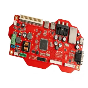
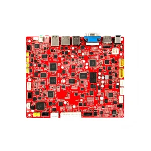
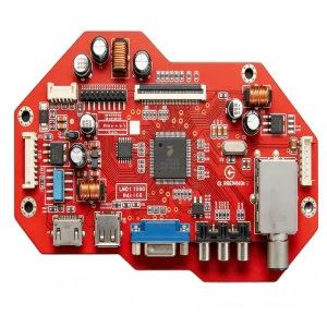
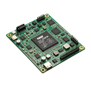
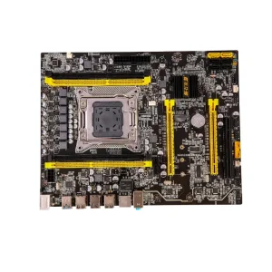
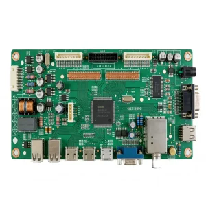
From micro-sensor instrumentation to high-speed communication switches, explore a selection of our industrial-grade, certified PCBA manufacturing solutions.
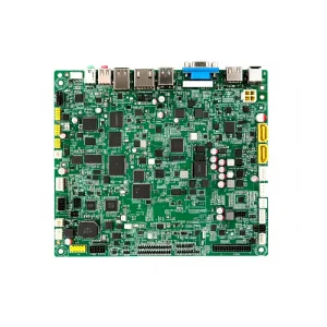
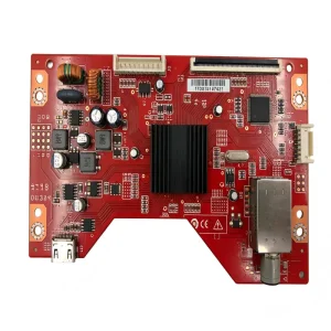
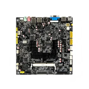

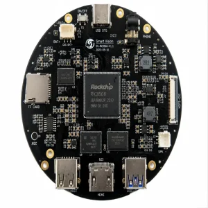
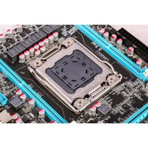
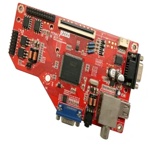
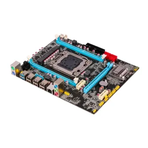
As electronic architectures converge around higher frequency, ultra-dense component packaging, and stringent thermal limits, printed circuit board manufacturing has transitioned from a commoditized fabrication task to an integrated physics-driven discipline.
The international printed circuit board market is experiencing relentless demand for High-Density Interconnect (HDI) boards. With consumer and industrial hardware integrating 0.35mm pitch BGAs and 01005 passives, standard multilayer boards are giving way to Any-Layer HDI, microvias with laser direct imaging (LDI), and copper-filled via-in-pad structures.
With the explosion of gallium nitride (GaN) power stages, electric vehicle (EV) charging stations, and industrial motor controllers, boards must dissipate extreme heat fluxes without thermal warping. This necessitates heavy-copper laminates (up to 6oz+), direct-bonded aluminum/copper metal cores (MCPCB), and precision embedded ceramic sinks.
Commercial standards are no longer adequate for regulated hardware. Autonomous driving sensors, implantable medical telemetry, and aerospace controllers mandate strict adherence to IPC-A-610 Class 3, IATF 16949 automotive standard, and ISO 13485 medical certifications with 100% automated optical and 3D X-ray inspection.
Dividing bare-board fabrication, semiconductor procurement, SMT assembly, and box-build across distinct geographic parties injects massive friction, compounded logistics tariffs, and unresolvable defect disputes. Modern technology innovators demand end-to-end, integrated Electronics Manufacturing Services (EMS) backed by deep traceability systems.
Shenzhen, and the greater Pearl River Delta, represents the densest electronics supply ecosystem on Earth. Here is how our modern Bao'an factory operationalizes this ecosystem to eliminate development cycles.
With instant access to 500,000+ active SKU part numbers and direct-tier access to global distributors (Digi-Key, Mouser, Arrow, Avnet) and domestic franchised suppliers, component turnaround that takes weeks in Western markets happens within 24 to 48 hours in Shenzhen.
Our internal staff of over 50 veteran engineers provides comprehensive Design for Manufacturability (DFM) and Design for Assembly (DFA) audits prior to tooling. We identify pad mismatches, insufficient solder dams, acid traps, and thermal imbalances before copper is etched.
Running 7 state-of-the-art SMT lines, 2 dual-wave DIP/THT lines, 2 selective soldering cells, and dedicated box-build workcenters, our workshop is instrumented with ERP and MES tracking down to individual component reels, solder paste lot numbers, and reflow profile curves.
Below is the audited production capability table maintained by STHL engineering, verifying parameters across fabrication, high-speed SMT assembly, and quality assurance.
| Capability Parameter | Standard Baseline | Advanced / Precision Limits | Inspection & Verification Method |
|---|---|---|---|
| Layer Count (Rigid) | 1 – 16 Layers | Up to 48 Layers Multilayer | Micro-sectioning, Automated X-Ray Alignment |
| Special Board Types | FR-4 (Tg 130–170°C), CEM-1 | Rogers, Teflon, Ceramic, Polyimide Flex, Rigid-Flex, MCPCB | Laminate Dielectric Withstanding & TGA Analysis |
| Min Trace Width / Spacing | 4 mil / 4 mil (0.1mm) | 2.5 mil / 2.5 mil (0.065mm) | Laser Direct Imaging (LDI) + AOI Scanning |
| Min Mechanical Drill / Laser Via | 0.20 mm (8 mil) | 0.10 mm (4 mil) UV Laser Microvias | Optical Hole Checker, Cross-Section Analysis |
| Surface Finishes | HASL, Lead-free HASL, OSP | ENIG, ENEPIG, Immersion Silver, Immersion Tin, Hard Gold Plating | XRF Plating Thickness Gauge (ASTM B568) |
| SMT Pitch & Placement Min | 0402 passives, 0.5mm BGA pitch | 01005 (0402 metric), 0.3mm ultra-fine BGA, PoP (Package-on-Package) | 3D SPI (Solder Paste Inspection) + High-Speed Pick & Place |
| Board Thickness & Tolerances | 0.4mm – 3.2mm (±10%) | 0.2mm – 6.0mm (±5%), Controlled Impedance (±5% / ±7%) | TDR (Time Domain Reflectometry) Testing |
| Assembly Inspection Systems | Visual QA, 2D AOI | In-line 3D SPI, Dual 3D In-line AOI, 3D Real-Time X-Ray (AXI), Flying Probe | IPC-A-610 Class 2 and Class 3 Certified Standards |
Different hardware ecosystems impose fundamentally distinct stress parameters. Our production cells are tailored to handle specific operational environments.
From pulse oximeters and patient ward monitoring gateways to critical MRI RF coils, our ISO 13485 certified clean assembly workshops guarantee low-residue cleaning, ultrasonic de-fluxing, selective silicone conformal coating, and full sub-assembly electrical isolation.
Automotive grade infotainment head units, motor control units (MCUs), and high-voltage battery management systems (BMS) are manufactured under strict IATF 16949 frameworks. We prevent intermittent micro-cracks with nitrogen-assisted reflow soldering and comprehensive thermal shock testing.
Wind turbine controllers, solar micro-inverters, and DIN-rail industrial power units demand sustained durability under severe weather, vibrations, and high line voltage. We employ heavy-copper board construction, high creepage clearances, and automated potted enclosures for enduring ruggedness.
The next decade of electronics manufacturing is marked by artificial intelligence, mmWave communications, and eco-sustainable green chemical processing.
Deep-learning neural networks are deployed on AOI cameras to identify micro-bridging, voiding, and cold solder joints with zero false-calls. Factory MES predicts equipment maintenance before mechanical drift causes defective solder pastes.
With frequencies climbing past 28 GHz and 77 GHz radar domains, standard FR-4 gives way to PTFE-filled, hydrocarbon ceramic laminates with dissipation factors (Df) under 0.002. Precision etching ensures clean transmission line geometries and controlled skin-effect losses.
Global regulatory mandates (RoHS 3, REACH, WEEE) require zero-halogen formulations, lead-free low-temperature alloys (such as Bi-Sn formulations), and fully closed-loop wastewater copper recovery systems to lower the carbon footprint of electronic manufacturing.
International hardware buyers and chief procurement officers evaluate EMS suppliers on four non-negotiable vectors to mitigate risk, secure intellectual property, and guarantee line continuity.
Hardware blueprints, proprietary firmware, and BOM structures are legally guarded by enforceable bilateral Non-Disclosure Agreements prior to CAD/Gerber file release, with internal file encryption controls.
ERP/MES barcode integration binds every single finished circuit board to its exact SMT line timestamp, feeder roll, reflow thermal sensor data, and technician identification for immediate traceability in field recalls.
Our component engineering team actively flags End-of-Life (EOL), Not-Recommended-for-New-Designs (NRND), and long lead-time components during the quotation stage, proposing drop-in pin-compatible second sources.
Tier-one EMS suppliers must support prototypes with zero Minimum Order Quantity (MOQ) and scale smoothly to mass production on identical SMT feeder platforms without requiring redesign or line re-validation.
Clear, direct technical answers to assist global sourcing teams, hardware developers, and procurement managers in qualifying our factory capabilities.
Discover our comprehensive assembly capabilities spanning industrial wind power controllers, high-reliability telecom intercoms, and high-frequency medical MRI systems.