Explore our high-reliability printed circuit board assemblies spanning advanced power conversion, high-speed routing, and mission-critical embedded control hardware.
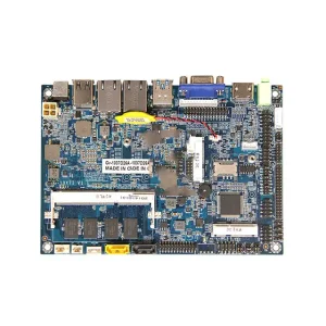
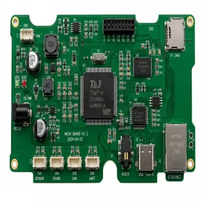

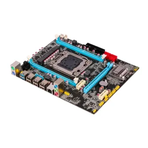
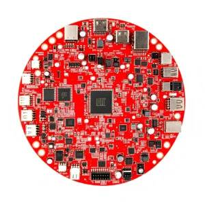
Analyzing global semiconductor integration, electrification trends, and the strategic distribution of rigid-flex and multi-layer board manufacturing capabilities.
The global printed circuit board fabrication industry is undergoing a structural transformation. Demand is pivoting rapidly from standard 2-to-6-layer FR-4 substrates toward high-density interconnect (HDI) microvia architectures, rigid-flex substrates, and high-frequency Rogers laminates. As edge-AI silicon and mmWave RF components compress footprint sizes, PCB bare board fabrication requires precision copper plating tolerances and fine-line etching below 2.5/2.5 mil line/space widths.
Global hardware innovators and tier-1 procurement divisions face recurring component obsolescence, localized raw material shortages, and fluctuating copper foil prices. Navigating this environment demands a manufacturing partner capable of turnkey component procurement and rapid substitute cross-referencing. STHL's direct integration with over 100 franchise distributor channels and certified mills ensures continuous production stability.
From RoHS 3 and REACH SVHC declarations to zero-halogen substrate specifications, environmental accountability governs modern fabrication. Operating within an accredited ISO 14001 framework, our Shenzhen manufacturing facility maintains closed-loop wastewater recycling, zero-discharge heavy metal recovery, and lead-free hot air solder leveling (HASL) & ENIG plating lines compliant with worldwide industrial standards.
How our strategic location in Bao'an District, Shenzhen, accelerates prototype-to-mass-production lifecycles for hardware engineering teams globally.
Situated in Bao'an, Shenzhen—the undisputed silicon capital of the world—STHL maintains immediate geographic proximity to Huaqiangbei's vast parts reserves and direct manufacturer component hubs. Passive pass-through components, exotic specialized sensors, custom connectors, and passive ceramic arrays can be procured, audited, and on the feeder line within 24 hours of RFQ release.
Decoupled contract manufacturing creates dangerous administrative delays, uncoordinated liability, and compounded markups. STHL eliminates third-party handoffs by unifying core bare-board PCB fabrication, multi-axis surface mount technology (SMT), through-hole assembly (THT/DIP), conformal spray coating, MCU firmware burning, and complete system chassis integration in one unified facility.
Every raw copper sheet, solder paste batch, and individual component roll enters our Enterprise Resource Planning (ERP) and Manufacturing Execution Systems (MES). Laser barcoding delivers full lot-level trace tracking from initial inner-layer imaging through pick-and-place placement to final flying probe and functional circuit testing.
Tailored bare-board fab parameters and advanced IPC-A-610 Class 3 assembly protocols built for hostile operating environments.
Heavy copper PCB fabrication (3oz - 6oz inner/outer layers) engineered to sustain high-current transient loads in EV on-board chargers (OBC), motor inverter controls, battery management systems (BMS), and autonomous driving LiDAR sensor suites. Stress-tested against thermal shock from -40°C to +150°C.
High-reliability, zero-defect fabrication for patient-connected monitoring equipment, portable smart blood glucose analyzers, intensive care ventilators, and surgical instruments. Verified through 3D automated X-ray inspection (AXI) to detect hidden BGA solder voiding below 10% threshold boundaries.
Ruggedized multi-layer boards manufactured with high-Tg FR-4 (Tg ≥ 170°C) and thick gold immersion plating (ENIG 3u") to endure chemical exposure, industrial vibration, and continuous power spikes across programmable logic controllers (PLCs), robotic gateways, and wind turbine pitch inverters.
Low-dielectric-loss Rogers and PTFE hybrid stack-ups supporting controlled impedance (+/-5%) and high-speed differential pairs up to 40Gbps. Serving enterprise 5G wireless repeaters, satellite voice recorders (CVR), microwave switches, and secure industrial IoT gateways.
Comprehensive engineering constraints, tolerances, and quality capabilities currently deployed across our Shenzhen production lines.
| Manufacturing Dimension | Standard Prototype Capability | Advanced Mass Production Limit | Verification & Test Methodology |
|---|---|---|---|
| Layer Count | 1 – 16 Layers | Up to 32 Layers (Blind / Buried Microvias) | Cross-sectioning & Metallographic Microscope |
| Supported Substrates | Standard FR-4, High-Tg (TG170/180) | Rogers, Aluminum Base, Polyimide (Flex), Rigid-Flex | IPC-TM-650 Thermal Stress Screening |
| Min. Trace Width / Spacing | 3.5 mil / 3.5 mil (0.09mm) | 2.5 mil / 2.5 mil (0.065mm) | Automated Optical Inspection (AOI) |
| Min. Mechanical Drill Hole | 0.20 mm (8 mil) | 0.15 mm (6 mil) / 0.10 mm Laser Microvia | Optical Hole Checker & X-Ray Coordinate Align |
| Controlled Impedance | ± 10% Standard | ± 5% Precision RF Matching | Polar CITS8800 Time Domain Reflectometry (TDR) |
| Surface Finishes | Lead-Free HASL, ENIG (Immersion Gold) | OSP, Immersion Silver, ENEPIG, Hard Gold Plating | X-Ray Fluorescence (XRF) Gold Thickness Gauge |
| SMT Component Pitch | 0402 Chips, 0.5mm Pitch BGA | 01005 passives, 0.3mm ultra-fine pitch BGA / QFN | 3D SPI (Solder Paste Insp.) + 3D AXI (X-Ray) |
| Traceability Framework | Lot-Level ERP Routing | Individual 2D Matrix Laser Mark + MES Data Trace | Full Lifetime Archival of Reflow Profiles & Test Logs |
How next-generation packaging, thermal dissipation physics, and AI automation dictate the next decade of electronic manufacturing.
With Wide Bandgap (WBG) semiconductors like Gallium Nitride (GaN) and Silicon Carbide (SiC) driving power supply densities upward, thermal dissipation has become the primary design hurdle. STHL pioneers advanced insulated metal substrate (IMS) solutions, embedded copper coin bonding, and selective thermal vias that drop junction temperatures by up to 28% compared to traditional FR-4 designs.
Human visual inspection is insufficient for 01005 passives and 0.3mm pitch micro-BGAs. Our automated SMT lines incorporate AI-driven 3D Solder Paste Inspection (SPI) directly networked with automated solder printers. Printing offsets are auto-corrected in real time, preventing 85% of downstream soldering defects before thermal reflow occurs.
Eliminating internal wire harnesses reduces device mass and catastrophic mechanical failure points. The convergence of dynamic flexible polyimide inner layers with rigid external FR-4 boards unlocks complex 3D assembly geometries vital for space-constrained medical implants, wearable robotics, and aerospace telemetry instruments.
A systematic framework for supply chain directors, VP engineers, and global procurement managers qualifying China PCBA vendors.
Trust begins prior to file release. Enterprise sourcing mandates executing bilateral Non-Disclosure Agreements (NDAs) that explicitly safeguard proprietary Gerber files, schematic diagrams, proprietary BOM pricing, and flashed firmware binaries. STHL enforces strict zero-leak internal engineering file segregation.
A premier manufacturer acts as an engineering extension, not a blind print shop. Our engineering team conducts deep Design for Manufacturability (DFM) and Design for Assembly (DFA) audits, catching aspect ratio flaws, thermal pad starvation, component shadow shadowing, and solder bridging risks before copper is etched.
Early-stage hardware development requires rapid 5-piece prototyping sprints; subsequent commercialization demands thousands of units per month. STHL provides a unified production ecosystem without Minimum Order Quantity (MOQ) penalties, allowing frictionless scaling without qualifying new suppliers.
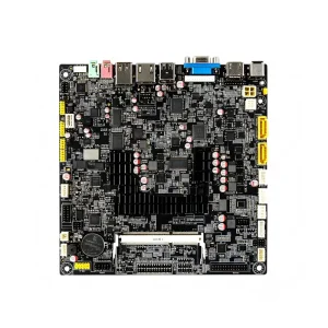
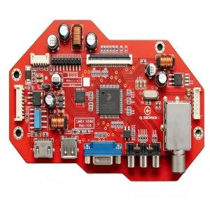
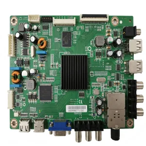
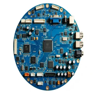
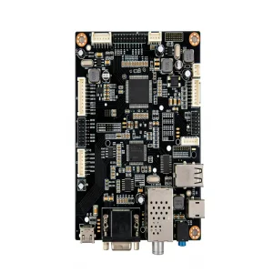
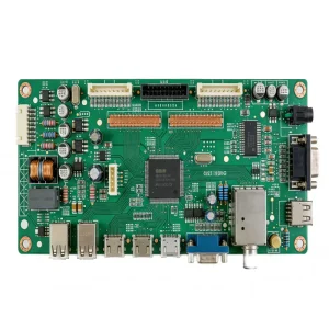
Verified hardware systems manufactured in our cleanrooms with full traceability and customized test fixtures.
Comprehensive answers direct from STHL's engineering and quality operations desks in Shenzhen.
