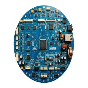
Industrial, sensing, optical, and high-frequency communication assemblies deployed across certified Tier-1 ecosystems.
De-risking electronic manufacturing lifecycles through deterministic SMT process windows, intelligent component traceability, and automated yield optimization.
Global procurement teams encounter systematic friction when dealing with fractured suppliers across bare-board fabrication, passives procurement, and assembly operations. Integrating bare board lamination with high-speed surface-mount technology eliminates finger-pointing and controls thermal shrinkage tolerances.
Counterfeit mitigation is an operational necessity. Direct API links with Tier-1 component aggregators alongside in-house scanning electron microscopy (SEM) and chemical decapsulation inspection guarantee that every pass-through active component matches OEM datasheet thermal characteristics precisely.
Miniaturization in medical optics, portable radar diagnostics, and edge IoT devices demands rigid-flex laser-drilled microvias down to 0.075 mm. Modern automated optical and X-ray systems audit copper plating thickness, aspect ratios, and void-free barrel fill profiles prior to solder reflow thermal excursion.
Every board passing through our facility undergoes systematic IPC Class 2 and Class 3 physical, chemical, and automated quality validation gates.
Pre-production valor audits parse Gerber, ODB++, and BOM matrices. Copper clearance, thermal relief pads, aspect ratio drill calculations, and component spacing undergo simulated validation to guarantee high fabrication yields.
Precision multi-layer lamination incorporates Rogers, Isola, and high-Tg FR-4 prepregs. Vacuum hydraulic presses calibrate heat profiles, eliminating delamination under rigorous automotive thermal cycling.
Dual-lane high-speed surface-mount placement robots achieve 01005 passives and 0.35 mm pitch micro-BGA positioning. 3D Solder Paste Inspection (SPI) calculates volumetric deposits down to micron tolerances.
Reflow profiles with 10-zone nitrogen atmospheres are strictly calibrated. Post-reflow inspection utilizes 3D AOI and multi-angle 3D X-ray (AXI) to identify voiding beneath thermal pads and BGA spheres.
Continuous facility evolution designed to conquer thermal dissipation thresholds, signal integrity losses, and heterogeneous system integration.
Eliminating regulatory hurdles across North American, European, and Asian destination ports through documented provenance.
STHL maintains continuous compliance with IATF 16949 for defect prevention within automotive supply chains, along with ISO 13485 regulating medical device PCBAs. Risk management files, PFMEAs, and IQ/OQ/PQ validations are standard for every program.
Full manufacturing lifecycle adherence to RoHS 3 and REACH mandates. Incoming wet chemical laboratories run ionic contamination tests (ROSE testing) to guarantee substrate cleanliness prior to selective conformal polyurethane or silicone coating.
Exporting to 90+ countries requires disciplined trade documentation. We handle specialized Harmonized System (HS) classifications, dual-use component clearances, and provide climate-controlled moisture barrier vacuum packaging (MSL Level 3/4 protection) with ESD bags.
Engineered to operate reliably under extreme temperature gradients, mechanical vibration, and continuous power load scenarios.
Definitive responses addressing design tolerances, counterfeit risk management, assembly yields, and global qualification parameters.
We deploy vacuum-assisted vapour phase reflow and custom multi-zone reflow convection ovens. Solder paste volume is strictly controlled with electroformed nickel-coated stencils, and all assemblies are audited with 3D transmission automated X-ray inspection (AXI) to maintain void rates below 10%, exceeding IPC-A-610 Class 3 limits.
Our centralized procurement team sources solely from franchised distributors and direct semiconductor fabrication partners. In-house verification features XRF spectroscopy for lead-finish confirmation, chemical decapsulation for die-marking audits, and electrical curve tracing to prevent compromised ICs from ever entering the feeders.
Yes. We operate specialized flexible NPI lines dedicated to prototype and low-volume production with no minimum order requirements. High-speed lines are matched to fast automated changeovers, allowing engineering design validation batches to transition into multi-thousand unit mass runs with zero parameter drift.
Every shipment includes an exhaustive Certificate of Conformance (CoC), IPC inspection reports, detailed AOI/AXI optical yield charts, thermal reflow profiles, and complete MES serial records detailing real-time reel-level component lots down to individual PCB tracking barcodes.