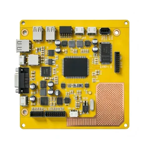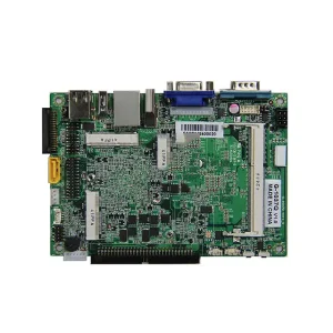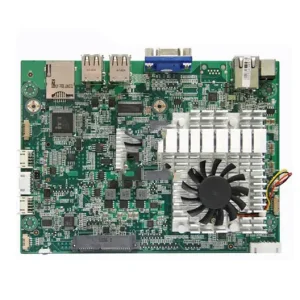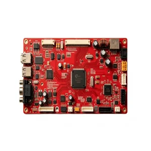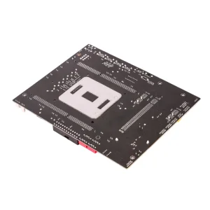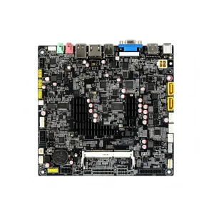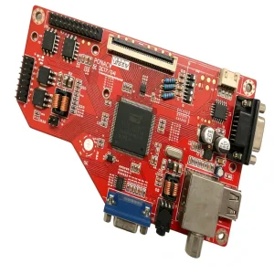
Explore high-complexity printed circuit board assemblies manufactured under strict defect-prevention protocols for medical, industrial, automotive, and mission-critical power systems.
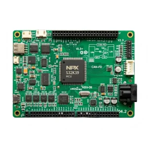
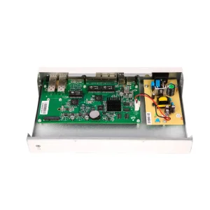
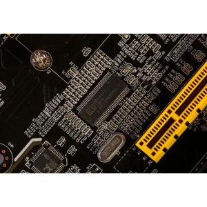
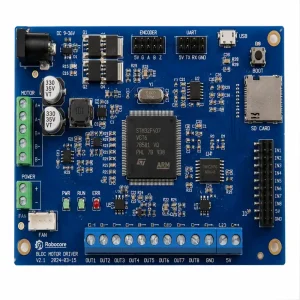
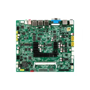

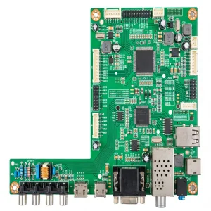
Shenzhen STHL Electronics Co., Ltd. (founded in 2006) operates an advanced electronics manufacturing complex located in Bao'an, Shenzhen. Staffed by 220+ technicians and 50+ engineers, we orchestrate closed-loop ERP and MES tracking from incoming raw CCL verification to high-density SMT and box build assembly.
High-speed Yamaha and Fuji pick-and-place lines supporting 01005 ultra-fine passives, 0.3mm pitch micro-BGA packages, package-on-package (PoP) placement, and active nitrogen-purged reflow chambers minimizing intermetallic voiding under 10%.
Real-time 3D Solder Paste Inspection (SPI), high-resolution Dual-Camera 3D Automated Optical Inspection (AOI), and high-voltage oblique-angle X-ray inspection to detect hidden solder bridges, head-in-pillow defects, and micro-cracking.
Direct API integrations with global franchised distributors including Arrow, Avnet, Digi-Key, Mouser, and verified original semiconductor fabricators, managing 500,000+ active parts with strict anti-counterfeit testing protocols.
A breakdown of the rigorous chemical, physical, and thermodynamic steps implemented across modern fabrication and assembly cleanrooms to ensure compliance with IPC Class 2 and Class 3 reliability standards.
Comprehensive design-rule check (DRC) reviewing Gerber RS-274X and ODB++ files. Engineers verify annular ring aspect ratios, trace-to-trace spacing, impedance matching line-widths, thermal relief geometry, and bill-of-materials (BOM) life-cycle viability under signed non-disclosure agreements (NDA).
Copper-clad laminates undergo mechanical cleaning, dry-film photoresist lamination, and Direct Optical Imaging (LDI). Laser-exposed inner copper layers are treated with chemical developing solutions and cupric chloride etchants, creating fine copper conductors followed by Automated Optical Inspection (AOI).
Inner copper layers are stacked with epoxy prepreg cores and outer copper foils, followed by high-temperature vacuum pressing at 185°C. High-speed CNC mechanical drilling and CO2/UV laser micro-via drilling create interconnect paths with micro-aspect ratios exceeding 10:1 for high-density multilayer boards.
Hole walls undergo permanganate desmearing and plasma etch to clear resin residue. Chemical electroless copper deposition coats microscopic non-conductive fiberglass walls with an ultra-thin 0.5–1.0 µm copper seed layer, preparing the panel for electrolytic acid copper pattern plating to ≥25 µm.
Liquid photoimageable (LPI) solder mask is coated, exposed, and thermal cured to insulate bare conductors. Boards receive specified high-performance surface finishes: ENIG (Electroless Nickel Immersion Gold), ENEPIG, Immersion Silver, OSP, or Lead-Free HASL for superior solderability and coplanarity.
Laser-cut stainless stencils and automated squeegee printers deposit lead-free SAC305 solder paste. 3D Solder Paste Inspection evaluates volume, height, and area before dual-gantry pick-and-place machines position 01005 passive chips, QFNs, and ball grid arrays with ±15µm accuracy.
Assemblies traverse a 10-zone reflow oven under controlled nitrogen (N2) atmosphere to mitigate oxidation, following tightly controlled thermal ramp, soak, liquidus (>217°C), and cooling slopes. Through-hole components are subsequently soldered using automated selective wave soldering machines.
PCBA units pass 3D AOI and 3D X-ray (AXI) for BGA solder joint verification. Boards undergo In-Circuit Testing (ICT), Flying Probe, custom functional testing (FCT), automated conformal coating against moisture/salt mist, and mechanical box build assembly before ESD-shielded packaging.
How the convergence of automotive electrification, AI edge computing, high-frequency telecommunications, and supply-chain resilience is reshaping modern PCB and PCBA manufacturing standards worldwide.
As microprocessors migrate to 3nm and 4nm lithography nodes, PCB substrate geometries demand line-width and line-spacing (L/S) below 30µm/30µm. Modified Semi-Additive Processes (mSAP), stacked microvias, and Any-Layer HDI architectures allow ultra-miniaturized electronics with higher signal integrity and reduced parasitic capacitance.
Global procurement teams prioritize tier-1 EMS providers capable of mitigating single-source chip shortages. Through active engineering alternatives, direct franchised distributor networks, and transparent cost-breakdown structures, OEMs avoid costly production line stoppages and hedge against unexpected geopolitical tariffs.
With widespread 5G mmWave infrastructure, LiDAR, and satellite IoT communications, factories must master hybrid laminates integrating PTFE, Rogers RO4350B, and Megtron 6 with heavy copper cores. Engineering controlled dielectric constants (Dk) and low dissipation factors (Df) ensures minimal insertion loss at frequencies above 40GHz.
From life-supporting biomedical electronics to harsh automotive engine compartments, STHL formulates custom manufacturing protocols adapted to your application's regulatory and operational demands.
ISO 13485-certified cleanroom lines producing pacemaker controls, diagnostic imaging workstations, and infusion pumps. Complete lot tracking, biocompatible conformal coatings, and 100% functional validation guaranteeing zero field-failure tolerance.
High-reliability assemblies for Battery Management Systems (BMS), Supplemental Restraint Systems (SRS), and DC-DC onboard chargers. Engineered to endure continuous thermal cycling (-40°C to +125°C), high mechanical vibration, and heavy current loads.
Heavy copper circuitry (up to 6 oz), high-voltage isolation barriers, and thick conformal coatings for photovoltaic inverters, industrial waste-gas monitors, and factory robotics exposed to airborne corrosive gases and electromagnetic interference.
Miniaturized rigid-flex and flex-PCB interconnects for surveillance cameras, smart intercoms, and connected garage door systems. Ultra-low sleep-current testing and robust RF trace tuning for seamless Wi-Fi 6, Zigbee, and Sub-1GHz communications.
Transparent technical parameters verified by our Shenzhen manufacturing facility to support component engineers, hardware architects, and sourcing directors during upfront feasibility evaluations.
| Manufacturing Dimension | Standard Capability | Advanced / High-Precision Tolerance |
|---|---|---|
| Layer Count & Stack-up | 1 – 28 Layers (Standard FR-4, High-Tg 170°C) | Up to 48 Layers, Rigid-Flex, HDI 3+N+3, Any-Layer Microvia |
| Min. Line Width / Line Spacing (L/S) | 3.0 mil / 3.0 mil (0.075mm / 0.075mm) | 2.0 mil / 2.0 mil (0.050mm / 0.050mm via laser direct imaging) |
| Minimum Mechanical Hole Size | 0.20 mm (8 mil) with 10:1 Aspect Ratio | 0.15 mm (6 mil) mechanical; 0.075 mm (3 mil) UV laser microvia |
| SMT Component Placement Size | 0201 passives, SOIC, TSSOP, QFP, standard BGA | 01005 passives, 0.3mm pitch micro-BGA, Package-on-Package (PoP) |
| Finished Copper Thickness | 1/3 oz to 2 oz (Inner and Outer Layers) | 3 oz to 10 oz Heavy Copper for High-Power EV/Inverter boards |
| Surface Finishes Available | Lead-Free HASL, OSP, Immersion Tin | ENIG (Gold: 1-3u"), ENEPIG, Immersion Silver, Hard Gold plating |
| Impedance Control Tolerance | ±10% standard controlled impedance | ±5% tight RF impedance (Single-ended & Differential microstrip) |
| Testing & Inspection Methods | In-Line 3D AOI, 3D SPI, Flying Probe Test | 3D X-Ray (AXI), Boundary Scan, ICT Fixture, Custom Functional Test |
STHL bridges overseas engineering departments with real-time Shenzhen manufacturing execution, adhering to strict Western environmental standards and stringent IP safeguarding mechanisms.
Every incoming bill-of-materials undergoes material compliance scrubbing. We certify 100% lead-free, halogen-free, RoHS 3 (EU 2015/863), and REACH SVHC conformity, coupled with certified smelter conflict-mineral due diligence reports (CMRT) for Fortune 500 audit trails.
Strict Non-Disclosure Agreements (NDA) are executed prior to Gerber and schematic transmission. Our internal enterprise server enforces physical data isolation, role-based access control, and encrypted network transmission to guarantee complete design confidentiality.
Senior field-application and production engineers provide rapid, real-time responses across North American, European, and Asia-Pacific time zones. From early DFM feedback within 12 hours to live video factory audits, our communication is seamless and transparent.
Our Shenzhen factory systems undergo routine annual audits by certified international accreditation bodies, confirming strict process controls, product repeatability, and defect mitigation.
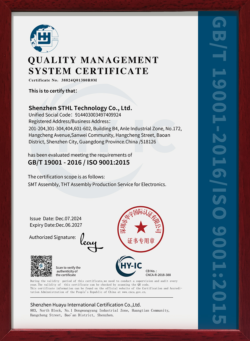
Global standard for comprehensive quality management system across fabrication, SMT assembly, and delivery.
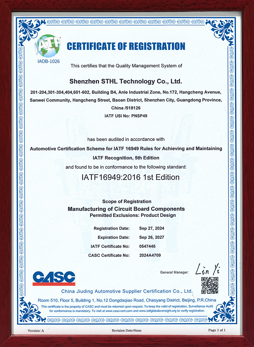
Automotive industry quality management system ensuring zero-defect mentality, FMEA, and PPAP Level 3 compliance.
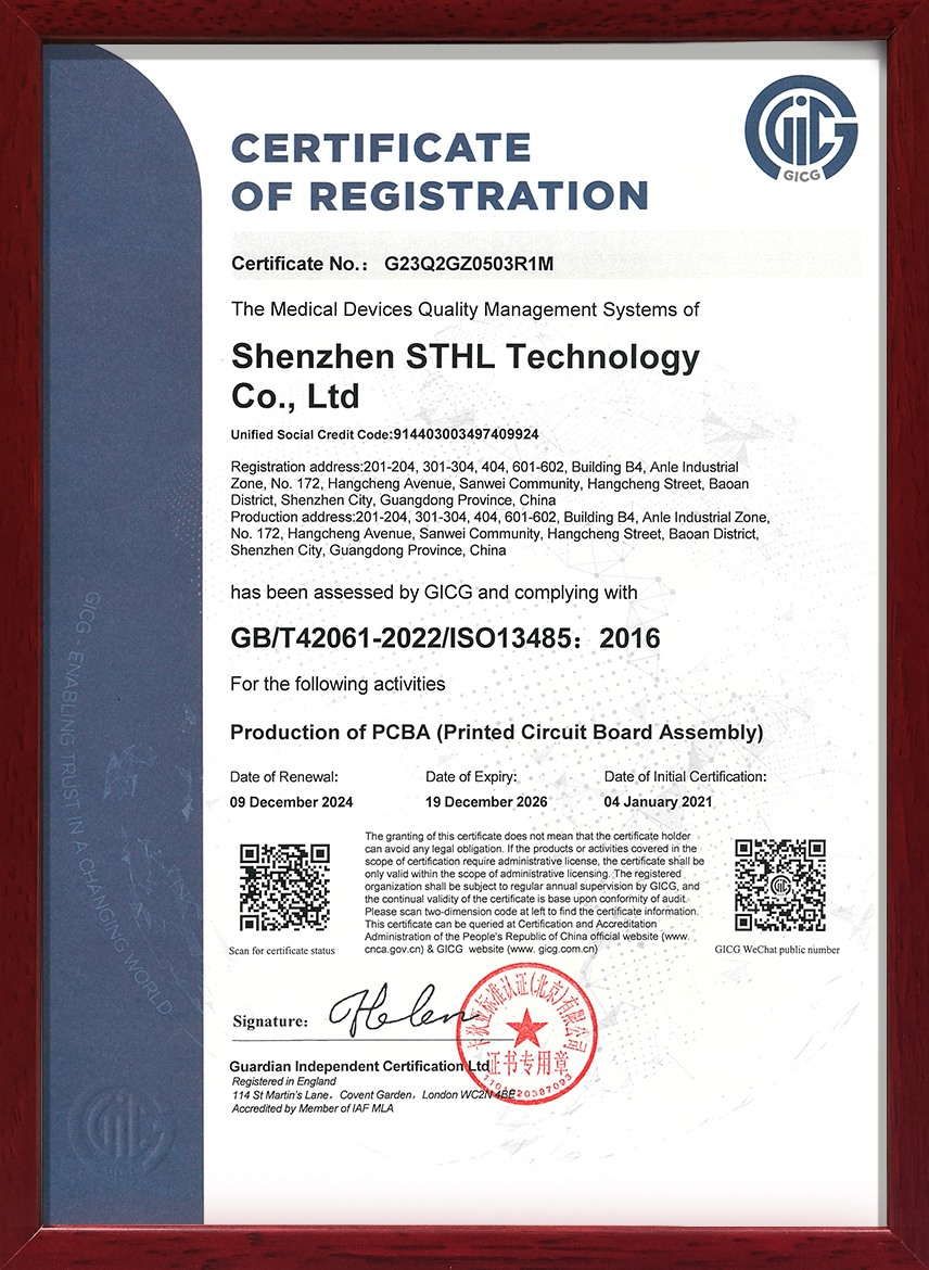
Rigorous medical device quality management standard governing device traceability and clean manufacturing environments.
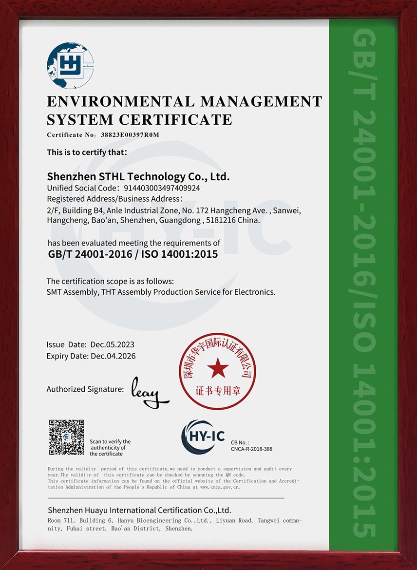
Environmental management system confirming responsible chemical recycling, waste management, and energy efficiency.
Continuous investment into automated semiconductor substrate packaging, AI visual classification, and additive green chemical fabrication processes through 2026 and beyond.
Integrating deep-learning neural networks into inline 3D AOI and 3D AXI inspection stations. Machine learning models distinguish cosmetic pseudo-defects from true solder fatigue cracks, boosting first-pass yield (FPY) by 18% and preventing escape defects to field operations.
Transitioning beyond discrete 0201/01005 surface mounts by burying thin-film resistors and planar capacitors directly inside laminate core dielectric layers. This eliminates surface routing bottlenecks, optimizes high-speed signal pathways, and enhances EMI shield efficiency.
Pioneering automated closed-loop copper extraction from chemical micro-etching solutions. Advanced zero-liquid-discharge (ZLD) wastewater reclamation facilities enable STHL to reuse 90% of industrial process water, supporting OEM corporate carbon-neutrality mandates.
Direct endorsements from R&D engineers, hardware architects, and executives across the United States, Germany, Italy, and international high-tech clusters.
"Excellent team to work with and fast delivery with high-quality boards. We are very happy to work with such a good supplier. Thanks again."

"Please extend my thanks to your team for the hard work in preparing these samples. This experience has strengthened my confidence in your company, and I look forward to discussing bulk orders soon."

"We are satisfied with the last order. You did a great job on those boards and the lead time was short. I will place a new order soon."

In-depth responses to technical inquiries regarding manufacturing capabilities, component integrity, DFM workflows, lead-times, and quality assurance.
Explore our extensive track record of mission-critical assemblies engineered for renewable energy systems, environmental diagnostics, medical monitoring, and robust AC/DC conversion.