Engineered for extreme operating environments, our SMT and THT fabrication modules maintain IPC Class 3 compliance across mission-critical automotive, smart infrastructure, and heavy industrial controls.

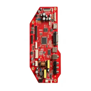

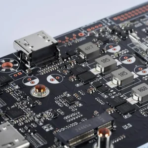
Evaluating electronics manufacturing service (EMS) partners requires a shift from superficial piece-part costing to holistic Lifecycle Total Cost of Ownership (TCO) modeling.
In modern industrial electronics procurement, sourcing directors face escalating pressure to balance geopolitical risk, volatile lead times, and microscopic geometric tolerances. Contracting with a true tier-1 PCB printing manufacturer & factory is no longer simply about acquiring etched copper boards; it is a long-term strategic alignment determining product yield, regulatory speed-to-market, and field longevity. Whether managing medical diagnostics or high-power industrial inverters, system failure is non-negotiable.
Direct bare-board costs represent less than 15% of complete assembly liability. Unbudgeted expenses arise from cold solder joints, component obsolescence re-spins, late deliveries, and field warranty claims.
Direct API-linked component procurement channels spanning Mouser, Digi-Key, Arrow, and Avnet ensure verified silicon authenticity, lot traceability, and dual-sourcing alternatives for critical ICs.
Enterprise procurement demands bulletproof data segregation. Rigorous non-disclosure protocols (NDAs), encrypted CAD handling, and isolated firmware flashing guarantee client IP confidentiality.
A resilient sourcing strategy insists on transparent DFM (Design for Manufacturability) and DFA (Design for Assembly) feedback before tooling commences. By scrutinizing trace-to-trace clearance, thermal relief balancing, drill aspect ratios, and stencil aperture geometry at the quoting stage, enterprise manufacturers prevent yield loss before a single ounce of copper is laminated.
Precision PCB printing integrates chemical photolithography, high-speed pick-and-place automation, vacuum reflow soldering, and multi-spectral inspection arrays.
The boundary between bare circuit board printing and final electromechanical assembly has collapsed. Today’s high-density interconnect (HDI) designs require deep synergy between substrate lamination thermodynamics and surface mount component placement accuracy. Leading-edge PCB printing factories employ computerized laser direct imaging (LDI) to resolve conductor geometries below 3 mils (75µm), eliminating visual distortion and misalignment on expansive multi-layer panels.
| Process Parameter | Standard Capability | Advanced / High-Density Interconnect (HDI) | Validation Protocol |
|---|---|---|---|
| Layer Count Range | 2 – 16 Layers (FR-4 Standard / High-Tg) | Up to 32 Layers (Any-Layer HDI, Rigid-Flex, Polyimide) | Microsection Analysis / Layer Registration X-Ray |
| Min. Line Width / Trace Spacing | 0.1mm (4 mil) / 0.1mm | 0.065mm (2.5 mil) / 0.065mm | Laser Optical Measurement / AOI Automated Scan |
| SMT Placement Pitch & Size | 0402 Imperial (1005 Metric), 0.5mm Pitch QFP | 01005 Imperial (0402 Metric), 0.3mm Pitch BGA / CSP | 3D Solder Paste Inspection (SPI) + In-line AOI |
| Solder Reflow Environment | Multi-Zone Forced Convection (Lead-Free Sn-Ag-Cu) | Vacuum Atmosphere Reflow (Voiding < 5% under BGA pads) | Real-time KIC Thermal Profiling & Micro-void X-Ray |
| Surface Metallurgy | HASL Lead-Free, OSP, Chemical Tin | Electroless Nickel Immersion Gold (ENIG), ENEPIG, Hard Gold | XRF Coating Thickness Verification / Solderability Test |
High-reliability PCBA performance depends upon mitigating internal thermal-mechanical shear stresses. Through-hole plating must withstand repeated thermal excursions during soldering and real-world cycling without barrel cracking. By maintaining rigid copper barrel thickness standards exceeding 20–25µm inside plated through-holes (PTH), our factories guarantee uninterrupted signal continuity even under high vibrational shock.
Differential pair routing and controlled-impedance traces (±5% to ±10% tolerance) simulated with Polar Si8000 boundary software, verified on coupon strips via TDR (Time Domain Reflectometry).
Utilizing vacuum hot presses with strict temperature ramp-up profiles to balance resin flow and glass transition states (Tg 150°C to 180°C), eliminating delamination risks.
Automated optical inspection flags component misalignment, tombstoning, and solder bridges, while 3D X-ray inspection detects hidden voiding underneath dense BGA and QFN packages.
From automotive powertrain controllers to high-bandwidth telecom routing and medical instrumentation, manufacturing requirements diverge into distinct technical verticals.
Severe thermal cycling, heavy copper busbars for battery management systems (BMS), high vibration resistance, and comprehensive PPAP documentation packages.
Absolute traceability to the individual component reel, conformal silicone/polyurethane barrier coatings, zero-clean ionic residue thresholds, and full FMEA controls.
High-voltage galvanic isolation, surge suppression, potting protection against corrosive chemicals, and continuous multi-year operational MTBF ratings.
Rogers / PTFE hybrid stack-ups, stable dielectric constants (Dk) at millimeter-wave frequencies, precise back-drilling to eliminate unused via stubs, and RF shielding enclosures.
The roadmap for PCB printing over the coming five years is defined by miniaturization, thermal density, and digital integration. As silicon switches to Wide Bandgap (WBG) semiconductors like Gallium Nitride (GaN) and Silicon Carbide (SiC), standard FR-4 fails to manage power densities exceeding 100W/cm². Advanced manufacturing requires adopting Direct Copper Bonded (DCB) ceramic substrates, insulated metal substrates (IMS), and embedded passive components to shrink interconnect parasitics.
Concurrently, the proliferation of Substrate-Like PCBs (SLP) manufactured via modified Semi-Additive Processes (mSAP) allows line widths down to 25µm. Paired with AI-augmented DFM engines that simulate reflow solder warpage across asymmetric copper weights, high-reliability factories are pushing first-pass yields above 99.8% on ultra-dense multilayer assemblies.
International trade compliance and industrial standards require strict operational adherence to global audit systems and environmentally clean chemistry.
Strict adherence to acceptability criteria for printed board assemblies. Every solder joint is evaluated for heel wetting, side overhang, barrel fill percentage, and coplanarity tolerances.
Certified under IATF 16949 (Automotive), ISO 13485 (Medical Devices), ISO 9001 (Quality Management), and ISO 14001 (Environmental Safety) across all manufacturing sites.
Full compliance with hazardous material restrictions (lead, mercury, cadmium, hexavalent chromium, PBBs, PBDEs) alongside flammability certifications under Underwriters Laboratories standard 94V-0.
Quality assurance is anchored in digital Manufacturing Execution Systems (MES). Every production batch receives unique 2D DataMatrix barcodes laser-etched onto individual breakout boards. This links the exact solder paste batch number, reflow thermal profile, pick-and-place nozzle assignment, and AOI optical signature directly to your enterprise serial record. In the event of a field anomaly, pinpoint root-cause isolation eliminates wide-sweeping, catastrophic recalls.
Proven manufacturing lines delivering robust build quality for optical transceivers, avionic flight computers, medical monitoring instruments, and environmental telemetry.

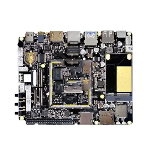
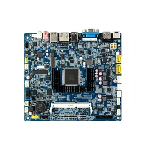


Authoritative insights directly addressing design qualification, high-reliability testing, lead times, and global volume manufacturing execution.
Industrial PCB manufacturing is characterized by tight trace width tolerances (±10% or better), controlled dielectric stack-ups, minimum 20µm hole-wall plating thickness, and IPC Class 3 quality gates. In contrast to low-cost consumer fabs, industrial-grade facilities enforce automated optical inspection (AOI) on all internal signal layers before lamination, utilize vacuum-assisted lamination presses to prevent micro-voiding, and provide certified material test reports verifying Tg (Glass Transition), Td (Decomposition Temperature), and CTE (Coefficient of Thermal Expansion).
We implement a zero-trust sourcing architecture. Active semiconductors and critical passive devices are sourced exclusively via franchised original component distributors (e.g., Arrow, Digi-Key, Mouser, Avnet) or directly from component manufacturers. Incoming lots undergo physical verification, including packaging moisture barrier bag (MBB) validation, external visual inspection under high-magnification microscopy, decapsulation spot-checks, acetone wipe solvent testing for re-marked parts, and X-ray fluorescence (XRF) elemental verification to guarantee pure RoHS lead-free compliance.
Because the solder interconnections of BGA, CSP, and bottom-terminated QFN packages are hidden beneath the component package, traditional optical cameras cannot confirm joint integrity. We deploy 3D Automated X-ray Inspection (AXI) to inspect every pad for voiding percentage (kept strictly under 10% to prevent thermal localized hotspots), solder ball sphericity, and bridge formation. Additionally, In-Circuit Testing (ICT) via bed-of-nails or flying probe fixtures verifies nodal continuity and passive values before boards transition to full functional electrical testing (FCT).
Fast-turn prototyping utilizes dedicated NPI (New Product Introduction) production lines segregated from high-volume batch runs. By employing frameless laser stencils, computerized jet-dispense solder printers, and multi-feeder pick-and-place heads capable of rapid feeder changeovers, prototype runs (1 to 50 boards) can complete assembly in 24 to 48 hours following component arrival. Crucially, prototype runs use identical reflow profiles and flux chemistries as high-volume lines, ensuring empirical qualification data translates seamlessly into volume production.
To execute an exhaustive DFM analysis and generate a turnkey quotation, clients should provide: (1) ODB++ format or standard RS-274X Gerber files including all copper, solder mask, silkscreen, and drill layers; (2) An unambiguous Bill of Materials (BOM) in Excel format containing Manufacturer Part Numbers (MPN), reference designators, package footprints, and secondary acceptable replacements; (3) Pick-and-Place Centroid data (X-Y coordinates and component rotation); and (4) Fabrication and Assembly drawings detailing board thickness, copper weights, solder mask color, surface finish (e.g., ENIG), and specific test requirements.
