Engineering Whitepaper & Industrial SMT Capabilities

High-Quality PCB SMD Manufacturer & Manufacturers

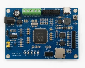
Pioneering turnkey surface-mount technology (SMT), ultra-dense component integration, automated micro-BGA placement, and rigorous IPC-A-610 Class 3 compliance for global high-reliability mission-critical electronics.

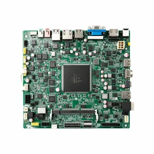
Featured SMT/SMD Applications

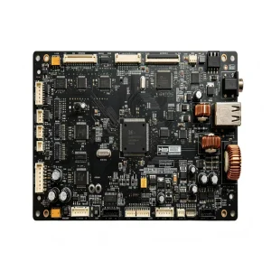
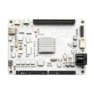
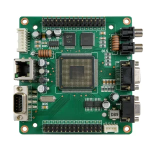
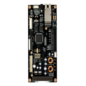
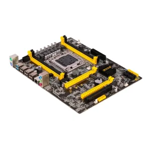
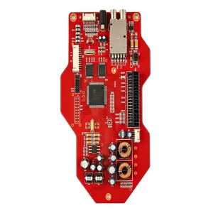
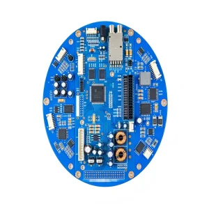
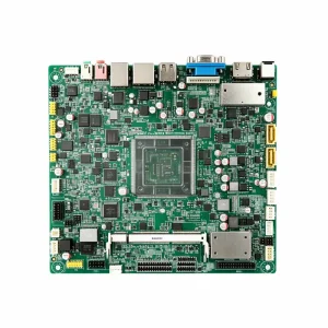
Precision Assemblies Manufactured Under Zero-Defect Standards

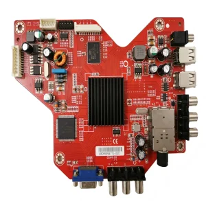
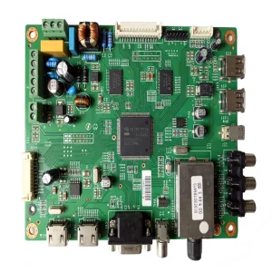
Engineered across automated surface-mount lines utilizing 10-zone reflow ovens, 3D SPI, and in-line automated optical/X-ray inspection to guarantee signal integrity, high current handling, and mechanical ruggedness.
Advanced Manufacturing Roadmap

State-of-the-Art Surface Mount Technology & Micro-Soldering Roadmap

Modern electronic hardware demands higher component density, tighter pitch limits, and strict thermal dissipation boundaries. Our manufacturing facilities incorporate Industry 4.0 automation to handle next-generation packaging formats with repeatable sub-micron precision.

Sub-Micron Micro-SMD & Ultra-Fine Pitch

As wearable devices and IoT edge modules shrink, component packages have evolved rapidly from 0402 and 0201 passives down to 01005 (0402 metric) and 008004 formats. Placing components measuring mere fractions of a millimeter requires specialized optical alignment, closed-loop linear encoder motor axes, and controlled electrostatic environments.

  • Placement accuracy down to ±15μm @ 3-sigma
  • Reliable pickup and alignment of 01005 and 008004 components
  • Fine-pitch IC support down to 0.3mm ball-pitch BGA, micro-CSP, and QFN
  • Nanocoated electroformed nickel stencils for crisp paste release

3D SPI & Solder Rheology Control

Over 65% of PCB assembly defects originate at the solder paste printing stage. STHL deploys in-line 3D Solder Paste Inspection (SPI) using dual-direction structured moiré light patterns immediately post-screen printing to inspect print height, volume, area, and bridging before any SMD component is placed on the board.

  • Real-time dynamic closed-loop feedback to automated printers
  • Automatic PCB offset compensation and squeegee pressure tracking
  • Stringent volume thresholds: 100% verification of QFN ground pads
  • Climate-regulated storage maintaining solder flux activity and viscosity

N2 Atmosphere Multi-Zone Reflow

Lead-free SAC305 and low-temperature alloys require strictly monitored thermal gradients. Our 10-heating-zone forced-convection reflow ovens operate under a continuous nitrogen (N2) purge atmosphere (<50 ppm oxygen), significantly reducing wetting angles, preventing intermetallic compound embrittlement, and eliminating oxidation.

  • 10 top and 10 bottom calibrated independent heating zones
  • Dual-rail architecture for mixed high-speed throughput
  • Peak thermal profile balancing ΔT across heavy copper planes
  • Integrated vacuum reflow chambers preventing void formation (<10%)
Operational Excellence

Scale, Engineering Muscle & Factory Capability in Numbers

Headquartered in Bao'an District, Shenzhen, STHL balances agility with high-volume capacity, maintaining end-to-end operational visibility under ERP and MES platforms.

20+
Years EMS Experience (Est. 2006)
10,000+
Square Meter Facility
7
High-Speed SMT Lines
50+
R&D & Process Engineers
99.5%
On-Time Delivery Rate
Macro Sector Engineering

Turnkey SMT Solutions Configured for Critical Industrial Sectors

Different operational environments present distinct physical, thermal, and regulatory hurdles. From functional safety in automotive braking to life-critical isolation in medical devices, our production gates are configured to satisfy strict international standards.

Automotive Electronics (IATF 16949)

Automotive PCBs must withstand constant harmonic vibration, severe thermal shock cycles (-40°C to +125°C), and high in-rush currents. Our automotive production processes strictly observe PPAP Level 3, incorporating automatic conformal coating, potting, and 100% automated optical and 3D X-ray validation.

  • Electronic Control Units (ECUs) and Anti-lock Braking (ABS)
  • Battery Management Systems (BMS) for hybrid & electric vehicles
  • Automotive LED lighting arrays and LiDAR/radar sensor packages
  • Full traceability to reel, lot, and machine feeder levels

Medical & Healthcare Instrumentation (ISO 13485)

Medical hardware cannot tolerate failure. STHL operates within ISO 13485 guidelines, ensuring that operating room visual monitors, laboratory automated diagnostic analyzers, and surgical tools possess verified dielectric clearances, low leakage currents, and complete device history records (DHR).

  • Class II & Class III medical monitoring board assemblies
  • Rigid-flex multi-layer circuits for portable point-of-care devices
  • IPC-A-610 Class 3 workmanship and strict cleanliness limits
  • Electromagnetic interference (EMI/EMC) shielded enclosures

Industrial Automation, Robotics & Smart Grid

Industrial equipment runs 24/7 in harsh operating atmospheres subject to electrical surges, moisture, and dust. We build high-copper-weight power distribution units (PDU), isolated DC-DC converters, PLC industrial controllers, and photovoltaic array monitoring systems with extended field operational lifespans.

  • Heavy copper PCB assemblies (up to 4oz–6oz outer/inner copper)
  • Automated selective soldering for mixed SMT/THT boards
  • Accelerated Environmental Stress Screening (ESS) and thermal burn-in
  • DIN-rail enclosure packaging, cable harness assembly, and test
China Factory 4.0 & Supply Chain Resilience

Shenzhen Ecosystem Powerhouse: BOM Agility & Scalable Delivery

Located in the world's primary hardware electronics hub, STHL connects global design houses with immediate engineering depth, direct component procurement pipelines, and rapid turnaround advantages.

Direct Tier-1 Silicon & Component Access

Mitigate single-source semiconductor choke points. Our certified component sourcing network maintains verified relationships with global distributors (Arrow, Avnet, Digi-Key, Mouser) alongside authorized domestic semiconductor foundries and passive manufacturers.

  • 500,000+ active parts verified through incoming IQC inspection
  • Real-time component counterfeit detection via X-ray & decapsulation
  • BOM scrub and lifecycle risk alerts for End-of-Life (EOL) passives
  • Pin-to-pin functional alternative cross-matching to optimize unit cost

Intelligent MES & Digital Batch Tracking

Our Manufacturing Execution System (MES) links automated surface-mount placement equipment, automated solder-paste screen printers, reflow temperature profiles, and visual inspection records into a singular, serialized work order database.

  • Laser-etched 2D DataMatrix code serialization per bare board
  • Machine parameter interlocking to prevent unauthorized setup changes
  • Instant reel-to-pad traceability for automotive and medical audits
  • Digital paperless SPC charting across solder defects, yields, and DPU

Flexible Scale: Prototypes to Mass Production

Avoid the operational friction of transferring an NPI (New Product Introduction) build between different prototype houses and volume manufacturers. STHL operates dedicated NPI quick-turn lanes alongside high-throughput automated lines.

  • Zero Minimum Order Quantity (No MOQ) for prototypes and pilot runs
  • Seamless engineering transition from 5 sample boards to 500k units
  • Turnkey box build, potting, wire cabling, and end-customer packaging
  • Consolidated customs clearance with express global freight dispatch
Rigorous Inspection & Compliance

Engineering Capabilities, Quality Systems & Tolerances

Compare our factory floor tolerances, equipment specifications, and quality controls to evaluate compatibility with your gerber layers, BOM requirements, and IPC class targets.

Manufacturing Parameter Standard Capability Advanced / High-Density Interconnect (HDI) Testing & Compliance Method
PCB Substrate Materials FR-4 (Standard Tg 140°C, Mid Tg 150°C) High-Tg (170-180°C), Halogen-free, Rogers, Ceramic, Aluminum metal-core, Polyimide flex IPC-4101D / UL 94V-0
SMD Component Pitch 0402 passives, 0.5mm IC pitch 01005 & 008004 passives, 0.3mm ultra-fine BGA, CSP, WLCSP High-Speed Optical Alignment
Layer Count & Board Thickness 2 to 16 layers, 0.8mm – 2.4mm thickness Up to 48 layers, Any-Layer HDI via-in-pad, 0.2mm ultra-thin flex to 6.0mm heavy backplanes Microsection Analysis
Minimum Trace & Spacing 4 mil / 4 mil (0.1mm / 0.1mm) 2.5 mil / 2.5 mil (0.065mm / 0.065mm) for high-density routing Laser Direct Imaging (LDI)
Surface Finishes HASL lead-free, Standard ENIG (1-2u" Gold) Heavy Gold ENIG (3-5u"), ENEPIG, Immersion Silver, OSP, Hard Gold Fingers (30u") XRF Coating Thickness Gauge
Solder Joint Quality Standards IPC-A-610 Class 2 (Commercial electronics) IPC-A-610 Class 3 / IPC-J-STD-001 (Automotive, medical, aerospace, industrial) Certified In-House IPC Trainers
Inspection & Verification Visual inspection, In-line 2D AOI 3D SPI, 3D AOI, 2.5D/3D X-Ray (AXI) laminar computed tomography for BGA voids <10% MES Serialized Logging
Quality Management Systems ISO 9001:2015, ISO 14001:2015 IATF 16949 (Automotive), ISO 13485 (Medical devices) certified facilities Third-Party Annual Audits
Strategic Sourcing & Procurement

Global OEM Procurement Strategy: Reducing Total Cost of Ownership (TCO)

Procurement leaders realize that the lowest quoting price per unit frequently turns into an expensive disaster if solder joints fail in the field, component lead times balloon, or engineering revisions stall production lines. STHL addresses cost management systematically.

Front-Loaded DFM & DFA Analysis

Before metal touches solder or machines begin placement, our 50+ engineers execute a comprehensive Design for Manufacturing (DFM) and Design for Assembly (DFA) scrub. We identify thermal relief inadequacies, tombstoning risks on asymmetric passives, component shadow effects during wave/reflow soldering, and insufficient fiducial clearance before production launches.

  • Reduction of design rev cycles and re-spins
  • Optimized panelization minimizing edge waste
  • Standardized component land pattern recommendations

Intellectual Property & NDA Protection

Proprietary schematics, custom firmware binaries, and system architecture are protected under strictly enforced non-disclosure agreements (NDAs). Our IT infrastructure implements air-gapped programming workstations, segmented internal network topologies, and biometric restricted floor zones for confidential prototype development.

  • Strict NDA signed prior to RFQ document review
  • Encrypted hex/binary firmware flashing stations
  • Secure scrap disposal and traceability of defective ICs

Integrated Testing & Functional Assurance

Shipping bare-functional boards creates massive support overhead overseas. We design customized functional test fixtures (FCT), bed-of-nails in-circuit testers (ICT), boundary scan systems, and simulated operating loads to validate analog voltages, digital communications, RF output power, and boot sequence integrity before crating.

  • Bed-of-Nails ICT checking resistance, capacitance, diode drop
  • Custom FCT firmware verification under full operating load
  • Dedicated RF test rooms for Bluetooth, Wi-Fi, and 4G/5G units
International Engineering Validation

What Global Hardware Directors & Sourcing Managers Say

Delivering zero-defect PCB assemblies across 90+ countries and regions. From high-mix low-volume medical prototypes to scalable industrial hardware.

"Excellent team to work with and fast delivery with high-quality boards. We are very happy to work with such a good supplier. Thanks again."
Paulo
Paulo R&D Engineer · United States
"Please extend my thanks to your team for the hard work in preparing these samples. This experience has strengthened my confidence in your company, and I look forward to discussing bulk orders soon."
Olivia
Olivia Hardware Engineer · Germany
"We are satisfied with the last order. You did a great job on those boards and the lead time was short. I will place a new order soon."
William
William CEO · Italy
"The order was perfect—exactly as specified, with top quality. Highly recommend this reliable supplier."
Dmitry
Dmitry CEO · Brazil
"Very fast delivery, professional supplier and professional product. We will place a new order very soon!"
Sohiab
Sohiab Hardware Engineer · Turkey
"We have tested all the boards and I am highly pleased. I will repeat my order soon. Thank you again for your excellent service."
Anna
Anna Sr. Hardware Designer · New Zealand
Technical & Commercial FAQ

Frequently Asked Questions for SMT / SMD Procurement

Detailed, engineering-backed answers addressing the most critical technical and operational questions asked by purchasing directors and hardware architects.

What specific files and documentation are required to quote and launch an SMD assembly project?
To provide an accurate, transparent, and prompt turnkey quote, we require: (1) Gerber Files / ODB++ Data: Standard RS-274X format containing all copper layers, silkscreen, solder mask, drill data, and mechanical outline. (2) Bill of Materials (BOM): In Excel or CSV format, detailing reference designators, exact manufacturer part numbers (MPN), descriptions, package types, quantities per board, and approved second-source alternatives. (3) Centroid / Pick-and-Place File: Including reference designators, X/Y coordinates, layer (top/bottom), and rotation angle in degrees. (4) Assembly & Test Instructions: Detailing functional test fixtures, IC programming firmware binaries, conformal coating masking zones, and specific IPC acceptance classes.
How does STHL ensure voiding remains under 10% on Bottom-Terminated Components (QFN, DFN, BGA)?
Large thermal ground pads on QFNs and power ICs entrap outgassing flux volatiles during reflow. We eliminate voiding through a four-stage process: First, during DFM, we window-pane the stencil aperture on ground pads to reduce solder volume by 20%–35% while providing venting channels for volatile escape. Second, we specify ultra-low-voiding Type 4 or Type 4.5 SAC305 solder paste. Third, reflow takes place in a nitrogen-inerted atmosphere (<50 ppm O2) with a prolonged soak zone between 150°C and 190°C to activate fluxes completely. Fourth, for mission-critical automotive or aerospace designs, boards are routed through vacuum-assisted reflow, drawing void levels reliably below 8%–10%, certified through 3D AXI X-ray laminar computed tomography.
Is there a Minimum Order Quantity (MOQ), and how is prototype-to-volume transition managed?
We operate with Zero Minimum Order Quantity (No MOQ). Customers can order as few as 1 to 5 boards for initial prototype proof-of-concept. Because our prototype NPI lines use the identical feeders, screen printers, reflow profiles, and automated optical inspection programs as our high-speed volume production lines, there is zero engineering recalibration required when scaling from a 10-piece pilot run to 500,000 units. All setup data, stencil files, and pick-and-place calibrations are securely preserved in our central MES database.
What countermeasures are implemented to prevent counterfeit and grey-market electronic components?
STHL maintains strict supply chain custody policies. All active semiconductors and critical passives are sourced directly through original manufacturers or authorized franchised distributors (e.g., Arrow, Avnet, Digi-Key, Mouser, Farnell). For mature or hard-to-find components requiring qualified secondary channels, incoming components must undergo comprehensive testing at our Incoming Quality Control (IQC) laboratory, including external visual inspection for remarking/resurfacing, X-ray inspection of internal lead frames and die structures, acetone swab testing, solderability testing per IPC/JEDEC J-STD-002, and decapsulation analysis.
What are the key differentiators between IPC-A-610 Class 2 and Class 3 assembly?
IPC Class 2 (Dedicated Service Electronic Products) covers commercial computing, consumer devices, and appliances where continued performance is expected but downtime is not catastrophic. IPC Class 3 (High Performance / Harsh Environment Electronic Products) applies to medical life-support, automotive functional safety, defense, and high-reliability industrial infrastructure where equipment downtime cannot be tolerated. In Class 3 assembly, solder barrel vertical fill for through-hole pins must exceed 75% (versus 50% for Class 2), surface-mount end/side joint overhang rules are significantly stricter, component alignment tolerances are narrower, and zero internal cleanliness residues or surface ionic contaminations are permitted.
How does STHL handle component obsolescence and supply-chain lead-time disruptions?
Our procurement team runs algorithmic BOM risk evaluations. When components hit End-of-Life (EOL), Notice of Discontinuation, or extended factory lead times (e.g., 26+ weeks), our hardware engineering staff proposes qualified drop-in alternatives, pin-compatible second sources, or minor layout re-spin options. We submit comprehensive comparison sheets (detailing electrical parameter overlaps, voltage tolerances, thermal footprints, and pricing) for client engineering sign-off before purchasing alternative silicon.
What international quality and process certifications govern STHL's manufacturing floors?
Our facility operates under rigorous international certifications: IATF 16949:2016 for automotive quality management and defect prevention; ISO 13485:2016 for medical device manufacturing and full DHR documentation; ISO 9001:2015 for organizational quality consistency; and ISO 14001:2015 for environmental control and RoHS/REACH substance compliance. All operators and quality inspectors are trained and certified to IPC-A-610 and IPC-J-STD-001 standards.
What testing fixtures and functional validation capabilities can be built in-house?
STHL maintains dedicated test engineering teams that design and mill custom mechanical test fixtures, including pneumatic clamp-down bed-of-nails In-Circuit Test (ICT) fixtures, micro-pogo-pin connector jigs, and custom Functional Circuit Test (FCT) consoles. We support automated firmware flashing via SWD/JTAG, CAN-bus / RS-485 / Modbus communication validation, RF output power calibration in shielded Faraday enclosures, high-voltage dielectric withstand (Hi-Pot) testing, and thermal chamber burn-in cycling.
Industrial & High-Reliability PCBA Portfolio

Explore Additional Specialized SMT Assembly Capabilities

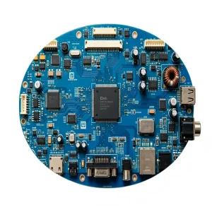
Featuring high-voltage power supplies, mission-critical environmental radiation sensors, ultra-compact RF communication equipment, and network video streaming devices.
Accelerate Your Hardware Delivery with STHL

Submit your Gerber files, Bill of Materials (BOM), and assembly criteria today. Our engineering department executes a comprehensive DFM audit, provides alternate component cost-saving proposals, and delivers a competitive quote within 24 hours under complete NDA protection.

Request an Engineering Quote (RFQ)