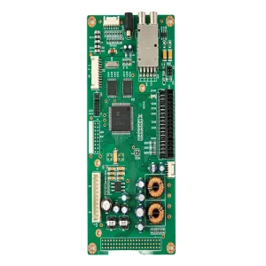
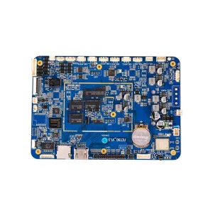
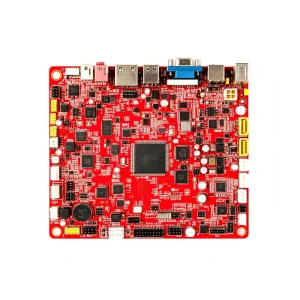
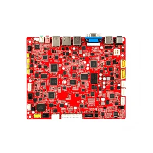
Explore our foundational turnkey manufacturing assemblies engineered for computer vision, smart energy management, industrial sensors, and mission-critical communications.
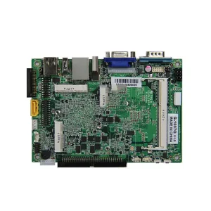
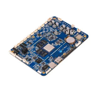
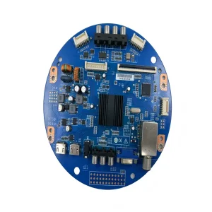
OEM Industrial Waste Gas Online Monitoring System PCB Assembly Service, Factories
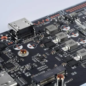
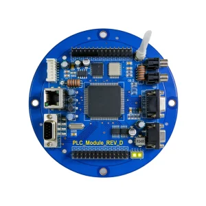
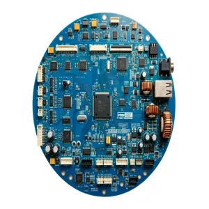
High-Quality Communication PCBA Application: Connecting the World with Precision Manufacturers, Factory
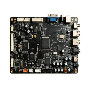
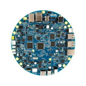
China In-vehicle Bluetooth Devices PCBA Assembly--STHL Manufacturer, Factories
Combining automated high-speed Panasonic/Yamaha SMT lines, ISO-certified cleanroom operations, and zero-defect quality culture to deliver Tier-1 contract electronic manufacturing.
Analyzing the paradigm shifts in surface-mount engineering, high-density interconnect (HDI) substrates, thermal dissapation management, and signal integrity for next-generation hardware.
The global printed circuit board assembly (PCBA) sector has transitioned decisively from simple contract assembly into an era of integrated electronic manufacturing services (EMS) governed by nano-scale component placement, high-density interconnections (HDI), and strict multi-domain regulatory standards. Modern hardware developers operating in industrial IoT, automotive electrified drivetrains, medical monitoring, and high-speed communications face severe engineering challenges: silicon dies are shrinking, operational frequencies exceed multiple gigahertz, and thermal envelope densities continue to intensify.
Achieving true high quality in printed circuit board assembly requires an interconnected manufacturing ecosystem where bare-board fabrication tolerances, chemical metallization consistency, precision solder paste rheology, high-speed pick-and-place precision, and multi-stage automated optical and radiographic inspections communicate seamlessly through an overarching Manufacturing Execution System (MES). At our Shenzhen facility, this closed-loop philosophy transforms design concepts into defect-free, deployable hardware solutions.
Over the past five years, four fundamental technical trajectories have redefined what constitutes a qualified Tier-1 PCBA assembly partner:
Placement of micro-passives down to 01005 and emerging 008004 chip formats requires optical centering systems with sub-15 micron repeatability, controlled stencil nano-coatings, and vacuum release automation.
Stacked microvias, laser-drilled blind and buried vias, and thin copper foil metallization ensure optimal propagation delay and impedance stability for 5G, RF modems, and edge AI compute platforms.
Utilizing multi-zone nitrogen reflow profiles and active vacuum reflow chambers reduces void ratios beneath power FETs and ground-slug QFNs below 8%, drastically surpassing IPC-A-610 Class 3 specifications.
How multinational OEMs overcome semiconductor obsolescence, lead-time volatility, counterfeit penetration, and tariff barriers through integrated supply chain partnerships.
Procurement directors and strategic sourcing managers face persistent supply chain friction. Unplanned component end-of-life (EOL) notifications, extended lead-time cycles on passive MLCCs and power management ICs, and the pervasive hazard of counterfeit components in open markets can halt assembly lines. A competent PCBA manufacturing partner must act as a strategic procurement buffer.
Our centralized procurement network in Shenzhen bridges direct factory allocations with authorized franchised distributors across North America, Europe, and the Asia-Pacific (including Mouser, Digi-Key, Arrow, Avnet, and original component manufacturers). By maintaining active BOM scrubbing and lifecycle health assessments during the initial Request for Quotation (RFQ) phase, we systematically identify supply chain vulnerabilities prior to production release.
Strict incoming material verification adhering to AS6174/IDEA-STD-1010 standards, incorporating decapsulation acid analysis, X-ray fluorescence (XRF) lead-finish verification, and solderability dipping tests.
In-house component engineering teams formulate pin-compatible drop-in replacements and redesign recommendations for high-risk single-source microcontrollers, LDOs, and interface transceivers.
Leveraging continuous rolling forecast models, safety stock agreements, and bonded warehouse reserves for high-consumption components ensures continuous delivery despite global spot-market shocks.
Upload your project BOM and Gerber package. Our component engineers deliver a full obsolescence risk report and DFM validation within 24 hours.
From fail-safe automotive ECUs to life-critical medical diagnostics, our tailored production ecosystems adapt precisely to individual sector compliance frameworks.
| Industry Sector | Core Compliance Frameworks | Manufacturing & Engineering Focus | Typical PCBA Implementations |
|---|---|---|---|
| Automotive Electronics | IATF 16949, AEC-Q100/200, ISO 26262 ASIL-D | PPAP Level 3 documentation, solder voiding < 10%, high-vibration thermal stress cycles, conformal silicone potting. | Electronic Control Units (ECU), Electronic Parking Brakes (EPB), Battery Management Systems (BMS), In-Vehicle Infotainment. |
| Medical & Healthcare | ISO 13485, FDA 21 CFR Part 820, IPC Class 3 | Full component lot-traceability, optical bio-sensor assembly, ionic contamination testing (< 1.56 μg/cm² NaCl equiv.), clean packaging. | Patient Monitors, Ultrasonic Imagers, Laboratory Waste Gas Analyzers, Wearable Medical Patches, Diagnostic Sensors. |
| Industrial Automation | ISO 9001, UL 508A, IEC 61010-1 | Heavy copper trace fabrication (up to 6 oz), galvanic isolation routing, robotic selective wave soldering, rugged DIN rail integration. | PLC Controllers, Variable Frequency Drives (VFD), Smart Grid Energy Meters, Industrial Gas Chromatography, Power Relays. |
| Telecommunications & RF | IPC-6012 Class 3, RoHS 3, REACH, CE/FCC | Controlled impedance matching (±5%), Rogers/Teflon hybrid laminations, RF shield-can automated soldering, high-speed eye diagram testing. | Industrial Wireless Modems, 5G Repeater Nodes, Video Surveillance Hubs, Optical Transceivers, Bluetooth Smart Gateways. |
| Clean Energy & Power | ISO 14001, IEC 62109, UL 94V-0 | High creepage and clearance design verification, thick dielectric FR-4, thermal aluminum core PCBs, high-voltage functional load testing. | Solar Microinverters, EV Wallbox Chargers, Linear Power Supplies, DIN Rail Switching Regulators, High-Efficiency LED Ballasts. |
Every single assembly passing through our facility is governed by strict stage-gate verifications, ensuring absolute defect containment prior to worldwide distribution.
Quality in electronic assembly is not inspected into a product; it is engineered into the manufacturing discipline. Operating under a multi-certified governance model encompassing IATF 16949 (Automotive Quality Management), ISO 13485 (Medical Devices Quality Management), ISO 9001, and ISO 14001, our Shenzhen manufacturing facility applies end-to-end computerized traceability. Every work order, SMT reel, solder paste jar, and rework operation is permanently indexed within our Enterprise Resource Planning (ERP) and Manufacturing Execution System (MES).
100% volumetric, height, area, and offset measurement of deposited solder paste immediately downstream of stencil printers, trapping over 70% of potential soldering defects prior to component mounting.
Multi-angle 3D Automated Optical Inspection verifies component polarity, tombstoning, and solder meniscus. High-resolution offline/inline 2.5D/3D X-ray systems audit BGA ball coplanarity and internal voiding.
Bed-of-nails flying probe and pneumatic bed test fixtures evaluate net impedances, followed by custom microcontroller flashing, automated RF signal validation, and extended environmental chamber burn-in.
Anticipating next-generation manufacturing requirements, our engineering facility continues to invest in emerging packaging architectures, intelligent shop-floor robotics, and eco-sustainable soldering chemistries.
The electronics hardware horizon is accelerating toward denser power-handling silicon, heterogeneous chiplet integration, and higher degrees of real-time operational feedback. Contract manufacturers who fail to adapt risk obsolescence. Our technology roadmap through 2030 centers around three transformation vectors:
Direct communication bridges between 3D SPI and automatic screen printers dynamically adjust stencil squeegee angle, speed, and separation stroke in real-time, autonomously neutralizing process drift.
Upgraded nitrogen reflow thermal profiles accommodate high-temperature solder alloys and copper sintering necessary for high-power Gallium Nitride (GaN) and Silicon Carbide (SiC) fast-switching topologies.
Full implementation of low-temperature soldering (LTS) alloys reduces reflow peak temperatures by 40°C, significantly shrinking factory carbon footprints while preserving delicate MEMS sensors and bio-materials.
In-depth technical answers addressing RFQ preparation, minimum order constraints, Design for Manufacturability (DFM) reviews, and proprietary intellectual property protection.
We require standard RS-274X or ODB++ Gerber files, a comprehensive Excel Bill of Materials (BOM) including original manufacturer part numbers (MPN), reference designators, and package descriptions, a centroid/pick-and-place (.txt or .csv) file with rotation angles, and detailed PCB fabrication drawings specifying layer stackup, impedance requirements, copper weight, and surface finish (ENIG, OSP, Immersion Silver, or HASL).
No. We operate with zero MOQ requirements. We specialize in high-mix, low-to-medium volume agile builds alongside mass production lines. Hardware teams can manufacture 5 to 50 prototype units for verification, transition seamlessly into pilot builds of 500 units, and subsequently scale to high-volume production of hundreds of thousands of assemblies on the exact same calibrated SMT equipment.
All client intellectual property is shielded under legally enforceable Non-Disclosure Agreements (NDA) prior to receiving design data. Firmware files are stored on isolated, encrypted engineering servers with strict role-based access control. IC flashing stations utilize secured automated programmers that record chip IDs, verify checksums, and lock programming bits to prevent reverse engineering or unauthorized firmware extraction.
Our Yamaha and Panasonic high-speed modular mounters handle micro-BGAs down to 0.3mm ball pitch, chip-scale packages (CSP), quad flat no-leads (QFN) down to 0.4mm lead pitch, and discrete passives down to 01005 sizing. Placement accuracy is verified through laser-alignment and prism optics at ±0.015mm, accompanied by 100% 3D Automated X-ray Inspection (AXI) to ensure absence of bridging, head-in-pillow defects, or excessive voiding.
Yes. Our turnkey value-added services include selective automated conformal coating (acrylics, silicones, polyurethanes, and UV-curable chemistries), two-part epoxy potting, wire harness and cable loom assembly, custom plastic injection-molded enclosure fitting, CNC-machined metal housing integration, and final consumer or retail gift-box packaging with drop-testing certification.
For quick-turn prototyping, bare boards and components can be assembled and shipped in as fast as 3 to 7 working days once all engineering clarifications (EQ) and parts are secured. Standard turnkey production runs typically require 2 to 3 weeks for complete bare PCB fabrication, component procurement, SMT/THT assembly, testing, and outbound logistics. Expedited emergency scheduling is readily available upon request.
Explore our specialized industrial assemblies covering precision automotive telemetry, healthcare diagnostic hardware, linear power regulators, and intelligent utility metering.
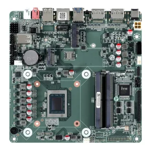
China Medical PCBA Application: Precision and Reliability for Healthcare Devices Manufacturer, Factories
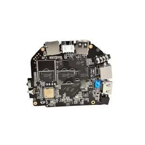
High-Quality Electronic Control Unit (ECU) PCB Assembly Manufacturers, Service