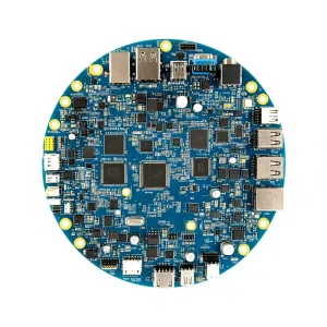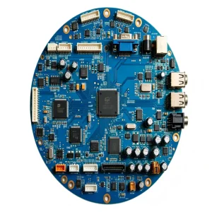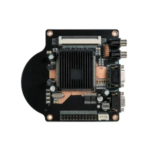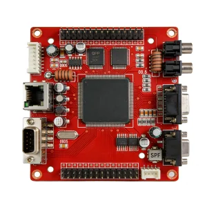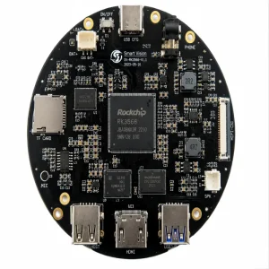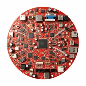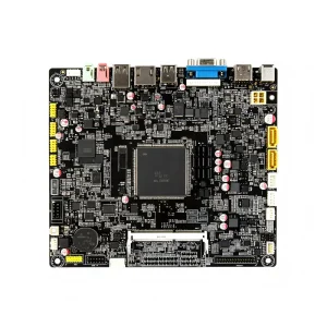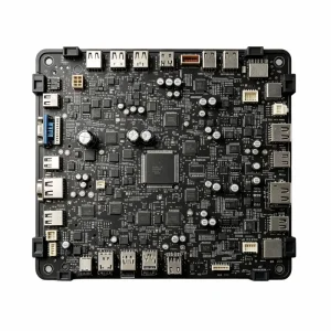
Explore high-yield turnkey solutions built with lot-level supply trace, rapid automated surface mounting, and rigorous parametric circuit screening.
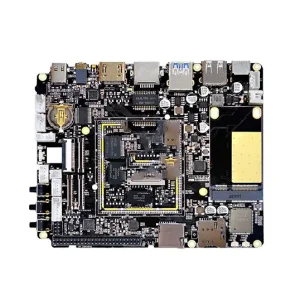
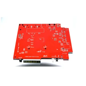

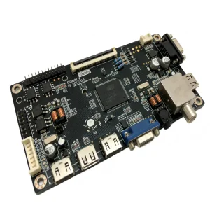
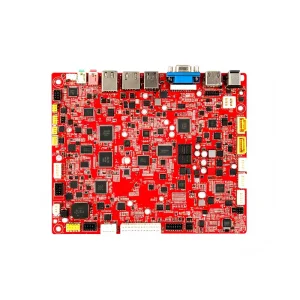
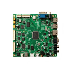
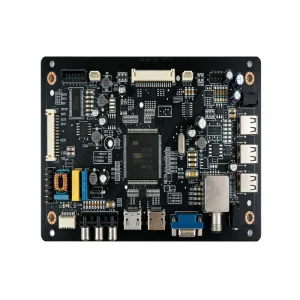
Shenzhen STHL Electronics provides full-stack EMS capabilities anchored by cleanroom manufacturing, automated optical inspection, and digitalized quality tracking.
Modern electronic assemblies are shifting toward higher frequencies, severe miniaturization, and mission-critical operating environments requiring specialized assembly protocols.
Micro-BGAs with ball pitches below 0.35mm and 01005 passives demand advanced multi-phase 3D Solder Paste Inspection (SPI) coupled with closed-loop precision stencil positioning to prevent bridging and solder starvation.
With silicon carbide and gallium nitride transitioning into mainstream automotive and renewable power electronics, thermal dissipation requires heavy-copper multilayer stackups, embedded copper coins, and vacuum reflow ovens.
Integration of machine learning algorithms within automated optical inspection platforms enables dynamic classification of solder meniscus consistency, eliminating false calls while securing genuine zero-escape quality for high-rel applications.
Supply chain leaders face unprecedented risks: unvetted gray-market counterfeits, erratic component lead times, and communication gaps between engineering and fabrication.
STHL partners directly with Tier-1 distributors including Digi-Key, Mouser, Arrow, Avnet, and original silicon fabricators. Every received active component undergoes incoming lot verification, decapsulation testing, and MES lot trace serialization.
Over 50 dedicated hardware engineers conduct upfront Design for Manufacturability (DFM), Design for Assembly (DFA), and Design for Testing (DFT) reviews prior to fabrication, proactively resolving non-standard footprints and reducing re-spin cycles.
Our rapid-response surface mount lines balance dynamic agility with industrial throughput. Hardware creators can manufacture prototype proof-of-concept runs without minimum order penalties and migrate seamlessly to high-volume assembly lines.
Eliminate supplier fragmentation and finger-pointing. We manage every phase from bare substrate fabrication to full functional testing and final carton packaging.
Access to over 500,000 active components through audited franchised distributors. Complete BOM scrubbing and proactive lifecycle alert systems for EOL parts.
Production spanning high-Tg standard FR-4, polyimide flex, rigid-flex, high-speed Rogers, ceramic substrates, and heavy copper configurations up to 32 layers.
High-speed Yamaha and Panasonic pick-and-place lines, nitrogen reflow, wave soldering, selective soldering, and complex fine-pitch BGA and LGA capabilities.
Automated conformal coating, ultrasonic plastic welding, cable harness assemblies, firmware flashing, and complete end-product functional system integration.
Every work order undergoes a rigorous, audit-ready workflow backed by enterprise ERP and MES systems for 100% board-level traceability.
Bilateral non-disclosure execution followed by comprehensive Gerber, centroid, and schematic engineering reviews.
Direct procurement via qualified authorized channels, incoming IQC lot testing, and climate-controlled storage.
Bare board production adhering to IPC-6012 standards, controlled impedance coupons, and flying probe testing.
Automated solder paste printing, 3D SPI, dual-lane chip mounting, reflow profiling, and selective pin-through soldering.
Multi-angle 3D AOI and 2D/3D X-ray analysis examining BGA voiding thresholds under 10% for mission-critical joints.
Custom bed-of-nails ICT, boundary scan, custom firmware flashing, and high-temp burn-in chamber environmental testing.
Conformal coating, anti-static moisture-barrier packaging with desiccant, and streamlined customs export to 90+ nations.
Delivering domain-specific electronics manufacturing optimized for environmental endurance, thermal stress, and long operating lifespans.
IATF 16949 certified PCBA for in-cabin communication, motor management, radar sub-assemblies, and LED lighting modules designed to withstand continuous vibration and extreme temperature shock cycles (-40°C to +125°C).
ISO 13485 compliant processes for patient monitoring equipment, analytical sensors, and handheld diagnostic electronics. Fully auditable DHR records, ionic contamination checks, and particulate-controlled cleanroom assembly.
Ruggedized PLC controllers, heavy-duty DIN-rail power modules, and intelligent IoT gateways engineered with thick conformal coatings to resist airborne chemicals, moisture, galvanic corrosion, and ESD events.
Inverter drive controls, solar micro-inverter boards, wind energy control units, and advanced Battery Management Systems (BMS) with high creepage and clearance routing up to 1500V DC operational ratings.
Clear manufacturing limits and process metrics for engineering teams conducting formal supplier qualification.
| Order Quantities & Model | High-Mix Low-Volume (HMLV), quick-turn prototyping, and high-volume mass production. No MOQ barriers. |
|---|---|
| SMT Component Placement | Passives down to 01005 (0402 metric), high-density BGA, micro-BGA, LGA, QFN down to 0.3mm pitch, POP (Package on Package). |
| Substrate Compatibility | Rigid FR-4 (Tg 130°C to 180°C), High-Frequency Rogers, Polyimide Flex, Rigid-Flex, Aluminum Core, Ceramic, Thick Copper. |
| Maximum PCB Dimensions | Single board up to 610mm × 500mm; Multilayer count up to 32 layers with controlled impedance (±7%). |
| Soldering Methods | Multi-zone Lead-Free Reflow, Convection Nitrogen Reflow, Dual-Wave Soldering, Selective Soldering, and Hand Micro-soldering. |
| Inspection & Verification | 3D SPI (Solder Paste Inspection), 3D AOI (Pre/Post-reflow), High-Resolution 2D/3D X-Ray Inspection, Flying Probe, ICT, and Custom FCT. |
| Quality Certifications | IATF 16949 (Automotive), ISO 9001:2015, ISO 13485 (Medical Devices), ISO 14001 (Environmental Management), IPC-A-610 Class 2 & 3. |
| Traceability & Governance | Full MES barcode serialization from bare PCB, incoming component reel lots, SMT feeder positions, to carton packaging. |
Ensuring complete legal certainty, data governance, and international customs compliance across global markets.
We execute legally binding non-disclosure agreements before receiving design data. Schematics, Gerber layers, and firmware hex binaries are housed on segregated internal servers with role-based access control and watermarked logs.
All turnkey assemblies strictly comply with EU RoHS 2.0 (2011/65/EU and 2015/863), REACH (EC 1907/2006) SVHC declarations, and Conflict Minerals reporting (CMRT) templates to guarantee seamless customs clearance across Europe and the Americas.
Direct freight consolidation partnerships with DHL, FedEx, and international air shipping agencies allow rapid door-to-door delivery with customs pre-clearance, providing customers in over 90 countries with transparent transit tracking.
Built upon enduring partnerships with world-renowned original component manufacturers and global Tier-1 distribution platforms.








Continuous investment in factory automation, digital twins, and advanced thermal substrate processing to support tomorrow's breakthrough innovations.
Expanding precision placement capabilities for ultra-thin SiP modules and bare silicon dies directly embedded alongside multi-layer organic interposers for next-generation edge devices.
Real-time thermodynamic profiling inside our reflow systems using finite element analysis (FEA) to accurately simulate solder behavior and eliminate thermal stress delamination in thick hybrid PCBs.
Targeting certified carbon-neutral cleanrooms by 2028 through closed-loop solvent reclamation, low-temperature alloy soldering techniques, and solar-assisted manufacturing infrastructures.
Detailed technical and operational answers to assist hardware developers and procurement directors during supplier audits.
Explore customized assemblies engineered for mission-critical environmental endurance, harsh industrial scenarios, and connected edge applications.