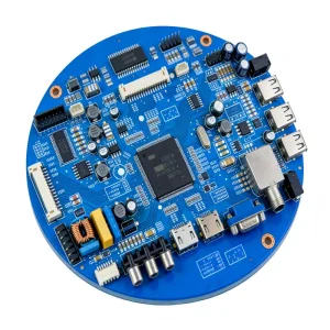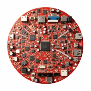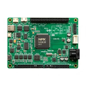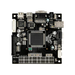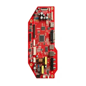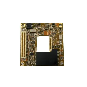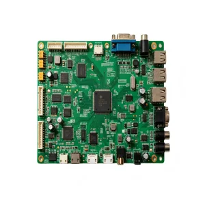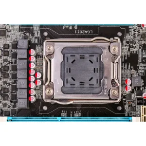
CT Scanner High-Precision PCBA Module
Explore CT Scanner PCB
Explore production-grade quick-turn PCBA modules manufactured to IPC-A-610 Class 3 and ISO 13485 / IATF 16949 standards for North American OEMs.
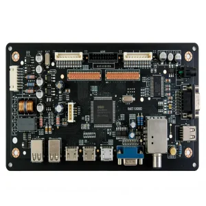
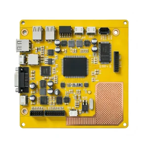

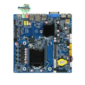
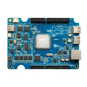
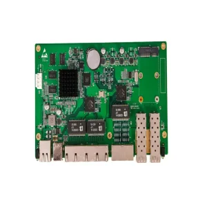
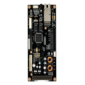
In modern electronic product design, speed-to-market is the defining metric of competitive advantage. American hardware innovators, aerospace contractors, and medical disruptors can no longer endure 8-week design validation cycles.
Global semiconductor allocations and fragmented bill of materials (BOM) pipelines stall North American engineering sprints. Our dual-channel sourcing ecosystem leverages trusted relationships with Mouser, Digi-Key, Arrow, and Avnet to secure hard-to-find microcontrollers, SiC switches, and FPGA packages instantly.
Every Gerber and ODB++ file uploaded undergoes automated AI and human cross-checked Design for Manufacturability (DFM) and Design for Assembly (DFA) audits. We catch trace-to-pad violations, solder-mask bridging hazards, thermal relief misalignments, and tombstone risks before bare board fabrication begins.
Prototyping is not simply making five boards; it is laying the mathematical baseline for seamless New Product Introduction (NPI). We configure machine placement programs, reflow profiles, and automated optical inspection (AOI) baselines that transition directly into mass production runs without requalification overhead.
Serving the United States engineering community requires absolute adherence to rigorous safety standards, component authenticity verification, and robust intellectual property protocols.
Proprietary topologies, custom FPGA code, and schematics represent your company’s core enterprise value. We execute comprehensive US-enforceable Non-Disclosure Agreements (NDAs) prior to receiving CAD data, backed by encrypted file vaults, isolated LAN servers, and compartmentalized operator access.
Our manufacturing floor operates under IATF 16949 (automotive), ISO 13485 (medical equipment), ISO 9001, and ISO 14001 certifications. Solder joints conform to IPC-A-610 Class 2 and Class 3 workmanship criteria, verified via 3D Automated Optical Inspection (AOI) and high-resolution X-ray inspection for BGA void control (<10%).
To ensure frictionless FCC certification and UL recognition, all prototype laminates (Isola, Shengyi, Rogers, Nelco) carry official UL94V-0 flammability certificates. Surface finishes—including Lead-Free HASL, ENIG (Immersion Gold), ENEPIG, and Immersion Silver—comply fully with EU RoHS, REACH, and California Proposition 65 directives.
Review our factory technical capabilities tailored to demanding R&D teams needing high-density interconnects (HDI), micro-BGAs, and specialized substrates.
| Technical Parameter | Quick-Turn Prototype Standard | Advanced / HDI R&D Capability |
|---|---|---|
| Layer Count Range | 1 – 16 Layers (Fast Turnaround) | Up to 48 Layers (Rigid, Flex, Rigid-Flex, HDI Any-Layer) |
| Minimum Trace / Space | 3 mil / 3 mil (0.075mm / 0.075mm) | 2 mil / 2 mil (0.05mm / 0.05mm) for ultra-dense packaging |
| SMT Component Pitch & Size | 0201 passives, 0.4mm pitch ICs | 01005 passives, 0.3mm BGA pitch, PoP (Package-on-Package) |
| Base Substrates | FR-4 (Standard & High-Tg 170-180°C) | Rogers 4350B, Nelco, Polyimide Flex, Heavy Copper (10oz), Ceramic |
| Via Technology | Standard Through-Hole, Tented Vias | Blind/Buried Vias, Laser Micro-vias, Via-in-Pad Plated Over (VIPPO) |
| Inspection & Testing Gates | Automated Optical Inspection (3D AOI), Flying Probe | 3D X-Ray (AXI), Functional Circuit Testing (FCT), Boundary Scan |
| US Turnaround Shipping | 24 to 72 Hours Fabrication + SMT | Direct DHL/FedEx Express Priority Delivery to any US address |
From the biotech corridors of Boston to the electric vehicle ecosystems of California, our prototype services satisfy demanding real-world operating environments.
FDA-aligned Class II and Class III medical prototypes, patient vital monitors, infusion pumps, ultrasound imaging, and non-invasive telehealth sensor hubs with high-Tg IPC-6012 Class 3 substrate reliability.
IATF 16949 compliant prototyping for Vehicle Control Units (VCU), BMS battery management boards, DC fast chargers, and LiDAR sensor processing cards engineered for harsh thermal shock and mechanical vibration.
High-layer count edge computing modules, industrial rack-mount power controllers, motor drive controllers, and telemetry nodes operating reliably in dirty, electromagnetically noisy factory environments.
Low-loss, impedance-controlled high-speed telecommunications prototypes utilizing Rogers RF substrates, matched-length differential pairs, and controlled dielectric constants for 5G, SATCOM, and radar arrays.
Prototyping technology is advancing rapidly. Here is how our engineering facility is evolving to support next-generation commercial hardware breakthroughs.
Deployment of sub-micron precision solder paste jet printers and high-speed mounters handling 01005 passives and 0.3mm pitch micro-BGAs without dedicated mechanical stencils.
Seamless integration of rigid-flex topologies with embedded passive components, thermal copper coins, and multi-laminate Rogers + FR-4 hybrids for compact IoT wearables.
AI neural networks trained on millions of soldering joints providing real-time void analysis, wetting angle verification, and internal wire-bond inspection for critical aerospace packages.
Adoption of low-temperature bio-flux soldering systems, 100% closed-loop aqueous board cleaning, and carbon-tracked raw material sourcing aligned with ESG compliance goals.
Straightforward answers regarding quoting, DFM analysis, component authenticity, shipping logistics, and intellectual property protection.
We offer an expedited 24- to 48-hour turn for bare board fabrication and 48- to 72-hour turnkey SMT assembly. With express international priority shipping via FedEx or DHL, boards typically clear customs and land on your US engineering workbench in 3 to 5 business days total.
We purchase directly from original component manufacturers (OCM) and tier-1 authorized distributors including Digi-Key, Mouser, Arrow, and Avnet. Every incoming reel is inspected for factory moisture barrier bags, barcoded lot traceability, pin-1 orientation, and date codes to guarantee authenticity.
Yes. We respect American corporate IP protection standards. We regularly review and sign mutual NDAs provided by client legal teams prior to accepting Gerber files, Bill of Materials (BOM), CAD centroid data, or firmware files.
To provide a firm price and DFM review within 2 to 12 hours, please supply: 1. Gerber (RS-274X) or ODB++ files, 2. Complete BOM (with manufacturer part numbers, descriptions, and quantities), 3. Pick-and-Place (Centroid / XY coordinates) file, and 4. Assembly drawings and programming/test notes.
From complex multi-channel smart displays to rugged power electronics, our proven assemblies reflect our 20-year track record of high-yield electronics manufacturing.