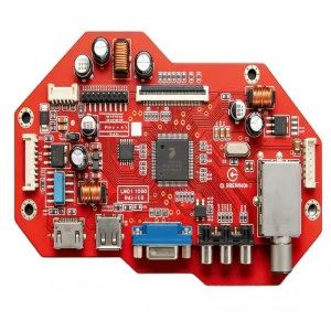
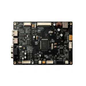
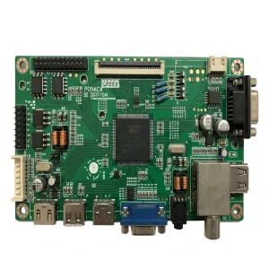
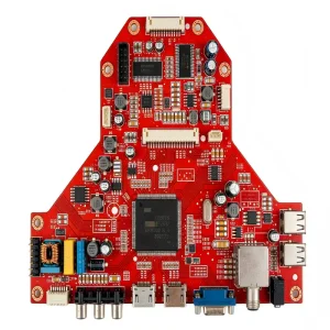
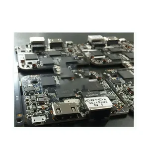
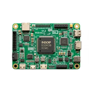
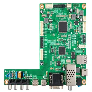
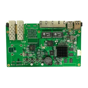
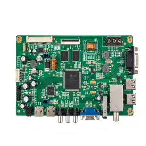
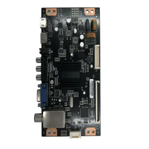
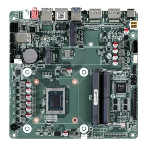
Explore engineering builds manufactured across our automated surface-mount lines, demonstrating high-mix component density, ruggedized packaging, and complete multi-layer verification.
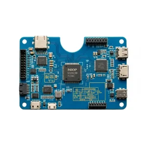
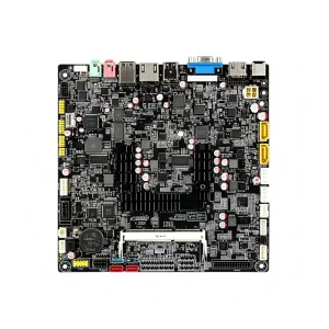
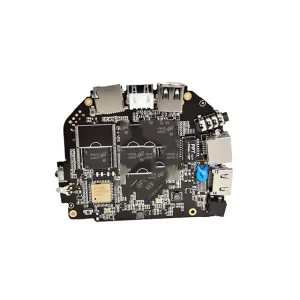
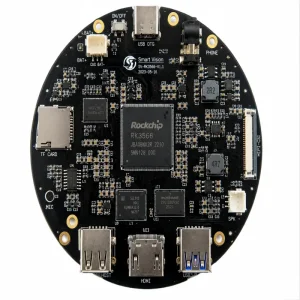
In modern electronic engineering, rapid prototyping is no longer merely a validation step—it is the strategic cornerstone of New Product Introduction (NPI), determining commercial time-to-market and post-launch reliability.
Global hardware innovators in automotive IoT, robotics, and medical therapeutics face shrinking revision windows. High-quality prototype SMT facilities bridge the gap between initial CAD layout and scalable volume production without engineering delays.
With silicon nodes shrinking, board real estate requires multi-layer blind and buried vias, micro-vias in pads, and ultra-fine pitch surface-mount packages. Modern prototype assembly demands production-grade placement accuracy down to ±15 microns.
Fabricating prototypes under lower-tier consumer standards risks masking fundamental design flaws. STHL enforces IATF 16949 and ISO 13485 quality baselines even for pilot batches of 5 to 50 boards, guaranteeing actionable validation data.
The geographic concentration of component manufacturers, PCB fabricators, and specialized test laboratories in Shenzhen creates an unmatched industrial velocity that compresses multi-month development cycles into days.
Through our established vendor matrix and close physical proximity to major silicon hubs, our engineering team sources hard-to-find passives, high-reliability ICs, and specialized connectors without cross-border customs bottlenecks.
Before laser stencils are cut, our 50+ staff engineers execute rigorous Design for Manufacturability (DFM) and Design for Assembly (DFA) audits, cross-referencing your Gerber, centroid, and BOM files to prevent cold solder joints or tombstoning.
China's mature tooling and precision stencil milling ecosystems lower NRE (Non-Recurring Engineering) expenses by up to 65% compared to North American or European facilities, allowing hardware start-ups to iterate multiple PCB spins affordably.
Validating pilot batches on our high-speed Panasonic and Yamaha modular pick-and-place lines ensures that feeding setups, feeder vibration profiles, and reflow recipes map 1:1 into mass production when orders scale to hundreds of thousands of units.
Comprehensive manufacturing capabilities engineered for high-density, high-reliability commercial, industrial, and medical grade electronics assembly.
| Manufacturing Parameter | Prototype / Quick-Turn Capability | Standard Production Tolerance | Advanced / Mission-Critical Capability |
|---|---|---|---|
| Minimum Component Size | 0201 (imperial) / 0603 (metric) | 0402 (imperial) | 01005 (0402 metric) & 008004 passives |
| BGA & CSP Ball Pitch | 0.4 mm minimum pitch | 0.5 mm – 0.8 mm pitch | Down to 0.3 mm pitch with micro-via-in-pad |
| Placement Accuracy | ±0.035 mm (±35 μm) | ±0.05 mm | ±0.015 mm (±15 μm) with optical alignment |
| Max / Min PCB Dimensions | 50 mm × 50 mm / 510 mm × 460 mm | Standard Eurocard / Custom panels | Up to 1200 mm × 300 mm (LED Longboards) |
| Layer Count Capability | 1 – 32 Layers (Rigid FR4) | 2 – 16 Layers | Up to 64 Layers HDI / Rigid-Flex Hybrid |
| Thermal Profiles Supported | Lead-Free SAC305, Sn-Pb Leaded | RoHS Compliant reflow profiles | Low-temp Bi-Sn / Step soldering profiles |
| Inspection Verification | 3D SPI + Inline 3D AOI | Automated Optical Inspection | 2.5D/3D High-Resolution X-Ray (AXI) & ICT |
From connected medical instrumentation to automotive chassis safety modules, prototype SMT assembly must satisfy demanding sector-specific operational criteria.
Precision monitoring hardware demands absolute thermal dissipation control and voiding ratios under 15% beneath exposed thermal pads. Our reflow systems utilize multi-zone profiling and nitrogen shielding to avoid solder degradation.
For powertrain controllers, Electronic Stability Programs (ESP), and telematics gateways, PCBA assemblies must withstand wide operating temperatures (-40°C to +125°C), demanding structural underfills and conformal coating protection.
Multi-gigabit network processors and industrial PoE injectors require strictly controlled 50Ω single-ended and 100Ω differential impedance traces, assembled with ultra-low flux residue to preserve signal integrity.
The electronic manufacturing industry is undergoing fundamental technological transformation, driven by artificial intelligence, smart manufacturing execution systems (MES), and extreme component miniaturization.
Modern SPI systems leverage neural networks to inspect volumetric solder deposition in real time, automatically compensating stencil printer wiper cycles and blade pressure to eliminate paste bridging before placement.
Every individual PCB is laser-etched with a unique 2D DataMatrix barcode. SMT pick-and-place feeders scan component reels, logging individual wafer lots, reflow oven thermal curves, and AOI images into an auditable manufacturing record.
For high-mix prototyping without dedicated stencil lead times, jet dispensing allows micron-level application of solder paste droplets, speeding up turn-around times to under 24 hours while supporting variable PCB cavity depths.
International procurement teams require clear guarantees regarding component authenticity, intellectual property security, and supply chain transparency when outsourcing prototype assembly.
All active ICs are procured strictly through factory-authorized franchised distributors (Digi-Key, Mouser, Arrow, Avnet) or original semiconductor manufacturers. Incoming lots undergo decapsulation testing, XRF material verification, and pin-scan checks.
Before schematic, Gerber, or firmware files are uploaded, an enforceable bilingual Non-Disclosure Agreement (NDA) is executed. Production engineering networks are air-gapped from external threats to safeguard proprietary IP.
Engineering departments should never be forced to commit to mass production run quantities during pilot stage debugging. STHL supports low-volume orders down to a single engineering unit, with identical production line quality protocols.
During initial quotation, our procurement specialists analyze BOM components for End-of-Life (EOL), Not Recommended for New Designs (NRND), and factory lead-time risks, recommending pin-compatible alternate silicon early.
Direct technical answers addressing the critical layout, testing, tolerance, and operational questions facing global hardware sourcing directors.
Explore additional turnkey production configurations delivered for smart metering, healthcare diagnostics, commercial LED illumination, and green energy management systems.

Send your Gerber files, BOM, and centroid Pick-and-Place data to our engineering team today for a confidential DFM feasibility review, line balancing simulation, and comprehensive quote within 24 hours.
