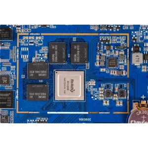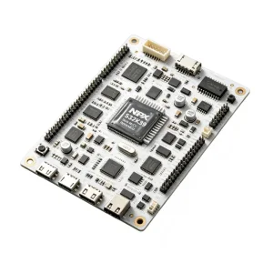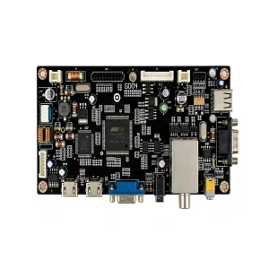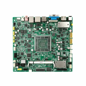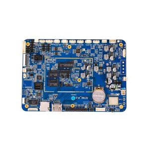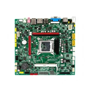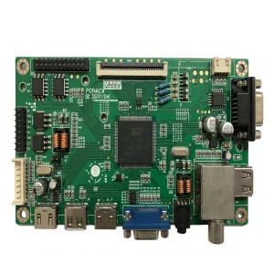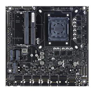
Explore engineering-grade PCB assemblies engineered under IPC-A-610 Class 2/3 specifications for high-stress aerospace, automotive, smart edge IoT, and mission-critical power systems.
Why modern hardware cycles demand an integrated, non-siloed approach bridging bare board fabrication, global components pipeline, and precision SMT mounting.
In high-velocity tech verticals, missing a market entry window by six weeks can degrade hardware profitability by up to 33%. Advanced quick turn PCB manufacturing compresses the traditional 4-week prototyping cycle into an agile 24 to 72-hour turnaround.
Speed without rigorous Design for Manufacturability (DFM) analysis leads to scrap. True engineering-centric factories apply full DRC and DFA checks the moment your Gerber, ODB++, and centroid files are parsed, catching layout anomalies before tooling strikes.
Dividing bare-board fab, component sourcing, SMT assembly, and test across different entities introduces logistical friction and accountability gaps. STHL unifies the complete electronics manufacturing life-cycle under an auditable, MES-tracked roof.
The Greater Bay Area (Shenzhen-Dongguan-Huizhou) houses the world's most concentrated microelectronics supply cluster, granting engineering teams unprecedented speed, component availability, and manufacturing agility.
Located in Shenzhen's Bao'an district, STHL accesses Huaqiangbei's massive component databases and authorized franchised distributors within hours, eliminating standard 2-3 week component procurement delays for hard-to-find passives, active MCUs, and memory chips.
Access immediate domestic inventory of high-grade copper clad laminates (Shengyi, Isola, Rogers, Panasonic Megtron) along with rapid tooling for flexible, rigid-flex, heavy copper (up to 10oz), and metal-core substrates under single-day turnaround parameters.
Leverage the structural cost efficiencies of Chinese production without sacrificing quality. Our high degree of automated optical inspection (AOI), 3D X-ray (AXI), and high-speed SMT placement delivers a 30-50% overall BOM and assembly cost reduction compared to EU/US factories.
Equipped with 7 high-speed SMT lines operating in rotating continuous shifts, STHL ensures prototyping never stops. Orders entering production in late afternoon undergo solder printing, surface mount, reflow, and inspection overnight, ready for testing at dawn.
Verified manufacturing parameters for precision prototyping, HDI microvias, and fine-pitch component mounting.
| Technical Parameter | Quick-Turn Prototype Standard | Advanced / Mass Production Tolerance | Quality Verification Protocol |
|---|---|---|---|
| Layer Count Capability | 1 – 16 Layers (24h - 48h express) | Up to 32 Layers / Multilayer HDI (1+N+1 to 3+N+3) | Cross-section microsectioning & impedance testing |
| Min. Line Width / Spacing | 3.0 mil / 3.0 mil (0.075mm) | 2.5 mil / 2.5 mil (0.065mm) for high-density interconnect | Automated Optical Inspection (AOI) |
| Min. Laser Drilled Via Size | 0.10mm (4 mil) microvias | 0.075mm (3 mil) stacked & staggered microvias | X-Ray inspection & barrel copper analysis |
| Surface Finishes | ENIG, HASL Lead-Free, Immersion Silver/Tin | OSP, Hard Gold, ENEPIG, Selective ENIG + Gold Finger | XRF plating thickness measurement |
| Component Packaging Range | 01005 chips, 0201, 0402, QFN, BGA (0.35mm pitch) | Micro-BGA, PoP (Package on Package), WLCSP | 3D SPI (Solder Paste Inspection) & 3D AXI (X-Ray) |
| Impedance Control | ±10% Standard single-ended / differential | ±5% Precision Controlled (Polar SI9000 validated) | TDR (Time Domain Reflectometry) coupon verification |
| Standard Certification | ISO 9001, RoHS, REACH compliant | IATF 16949 (Automotive), ISO 13485 (Medical Devices) | 100% In-circuit (ICT) and Functional Testing (FCT) |
The electronics manufacturing services (EMS) ecosystem is undergoing a generational shift catalyzed by high-speed communication standards (5G-Advanced and 6G R&D), edge Artificial Intelligence (AI) acceleration, and automotive electrification. High-frequency signaling demands materials with ultralow dielectric constants and dissipation factors (Dk/Df), transitioning conventional FR-4 substrates into customized PTFE and ceramic matrix blends. Quick-turn factories are no longer merely board-stuffing operations; they function as extended R&D arms, evaluating signal integrity (SI) and thermal dispersion on rapid iteration cycles.
Simultaneously, the convergence of Miniaturization and Power Density has mandated the deployment of embedded component technologies and rigid-flex configurations. Designers are consolidating complex multi-board cable assemblies into unified rigid-flex topologies to withstand dynamic vibration environments in robotics and in-vehicle applications. Factories capable of maintaining comprehensive inventories of low-Tg and high-Tg Polyimide flex materials—combined with automated laser cutting and precision registration tooling—are establishing irreplaceable moats in the global high-turnaround supply landscape.
At STHL, our engineering matrix is partitioned to address discrete compliance regimes and stress parameters across core industrial verticals:
Certified under IATF 16949, we supply quick-turn PCBA for Battery Management Systems (BMS), on-board chargers, and Vehicle Control Units (VCU). Thermal cycling endurance (-40°C to +125°C), conformal potting resistance, and automotive-grade PPAP documentation are integrated as baseline manufacturing procedures.
Operating in compliance with ISO 13485, our cleanroom assembly protocols safeguard biometric monitors, ultrasound processing units, and patient life-support boards against ionic contamination. Full lot-traceability maps every passive chip directly back to factory spool origins.
Addressing continuous duty cycles, high EMF environments, and surging currents. Our rapid assembly accommodates thick copper boards (3oz to 6oz outer layers), selective conformal coating against corrosive plant atmospheres, and high-voltage isolation slot milling.
Every work order traverses an automated MES-supervised pipeline that links engineering evaluation directly with shop-floor pick-and-place robotics.
Automated CAM scripts parse Gerber files, bill-of-materials, and centroid coordinates, catching pad geometry mismatches instantly.
ERP queries internal inventory containing 500,000+ line items; secondary pipelines trigger direct pull from franchised regional hubs.
Direct imaging, inner-layer etching, multi-layer pressing, laser drilling, and electrolytic copper plating execute in dedicated prototype lanes.
3D SPI validates solder paste deposition; dual-beam mounters place components at up to 80,000 CPH with laser alignment.
Multi-angle 3D AOI checks joint meniscus and polarity, while high-magnification AXI inspects under BGA solder balls for voids.
Custom flying probe checks or bed-of-nails test fixtures execute power-on simulation, firmware flashing, and clock verification.
Vacuum-sealed ESD moisture barrier packaging transferred to DHL/FedEx Express hubs for rapid customs transit to 90+ countries.
Procurement directors in Fortune 500 OEMs, Tier-1 automotive integrators, and medical device ventures share three primary concerns: supply chain resilience, counterfeit component elimination, and intellectual property confidentiality.
Our supply chain operates exclusively with authorized original component manufacturers and franchised global partners (Digi-Key, Mouser, Arrow, Avnet, Farnell). Incoming passive and active devices undergo inbound microscopy, lead frame inspection, and XRF material validation to protect your product from non-conforming or recycled silicon.
Engineering files, schematic drawings, firmware binaries, and BOM pricing schedules are treated as trade secrets. We execute bilaterally binding Non-Disclosure Agreements (NDAs) prior to data upload. All files reside in air-gapped internal servers with rigorous role-based permission tiers across our engineering group.
Through our integrated MES architecture, every single PCBA unit is assigned a laser-marked 2D DataMatrix code. This code links to reflow temperature profile curves, solder paste lot numbers, AOI visual inspection images, technician ID, and final functional test results, accessible for long-term audit compliance.
Expert answers addressing the practical considerations of rapid PCB fabrication, assembly turnaround, and prototype qualification.
For double-sided rigid FR-4 PCBs, our express fabrication cycle is 24 hours. Multilayer boards (4 to 8 layers) can be fabricated in 48 to 72 hours depending on complexity. For complete turnkey PCBA (PCB fab + component sourcing + SMT assembly), turnaround ranges from 3 to 7 business days, provided component availability is confirmed or parts are drawn from our extensive consigned/in-stock library.
Unlike prototype shops that use loose manual assembly methods, STHL runs rapid prototypes on the exact same high-speed SMT lines (Panasonic and Yamaha pick-and-place), precision stencil printers, and 10-zone reflow ovens used for high-volume automotive and medical production. Every board undergoes 3D AOI and X-ray inspection regardless of batch size, ensuring your pilot evaluation matches high-volume baseline yields.
To deliver an engineering review within 2 to 4 hours, we require: (1) Gerber RS-274X or ODB++ fabrication data; (2) A complete Bill of Materials (BOM) in Excel format with accurate Manufacturer Part Numbers (MPN) and approved alternate vendors; (3) Pick-and-place (Centroid/XY) coordinate file; and (4) Special assembly notes including layer stack-up, impedance tables, conformal coating outlines, and functional test specifications.
Yes. Our engineering procurement team continuously monitors component lifecycle states (EOL, NRND). If your BOM includes obsolete or long-lead items (e.g., 26+ week lead times), our hardware engineers propose drop-in pin-compatible replacements or form-fit-function equivalents from trusted domestic or international manufacturers for customer review before procurement.
We enforce No Minimum Order Quantity (No MOQ). We routinely manufacture prototype runs from 1 to 10 boards for hardware startups and corporate R&D groups, allowing engineering teams to rigorously validate proofs-of-concept before committing capital to full tooling and volume manufacturing.
Our bare PCB fabrication adheres strictly to IPC-6012 Class 2 and Class 3 specifications. All electronic assembly operations follow IPC-A-610 Class 2 standards by default, with Class 3 available for aerospace, military, and critical medical systems upon request. Solder alloys and chemical agents comply comprehensively with RoHS 3 (EU 2015/863) and REACH directives.
Broad industrial hardware categories successfully manufactured, programmed, tested, and boxed across STHL production cells.