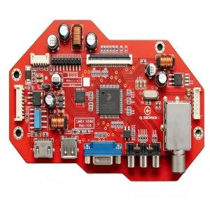
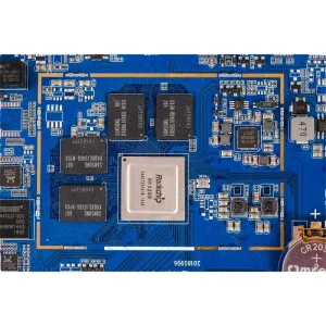
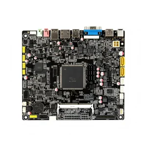
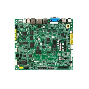
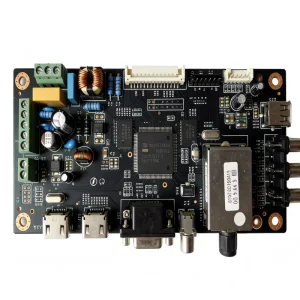
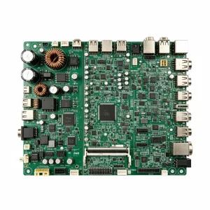
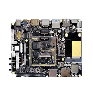
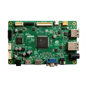
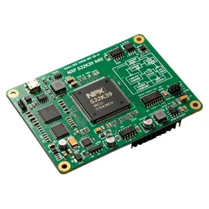
Featured quick-turn production runs engineered for demanding aerospace, automotive, medical, and industrial field deployments.
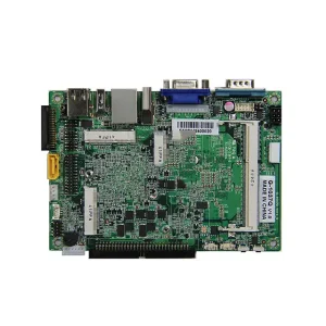
How Tier-1 original equipment manufacturers, hardware unicorns, and defense contractors solve the "Prototype-to-Mass-Production Valley of Death".
In modern electronic product engineering, rapid PCB prototyping has transitioned from a mere purchasing transaction into a strategic pillar of product lifecycle management (PLM). For multinational technology companies, engineering directors, and supply chain executives, the early new product introduction (NPI) phase represents the highest risk-reward inflection point. According to global research in electrical hardware systems, approximately 70% to 80% of total product manufacturing costs and long-term yield reliability are locked in during the early prototype design cycles. When prototype vendors overlook high-speed signal integrity, thermal dissipation topologies, or component obsolescence during the initial build, original equipment manufacturers (OEMs) face crippling respins, delayed market launch windows, and exponential redesign expenditures.
Global procurement teams operating in automotive ADAS, class-III medical devices, hyperscale telecom infrastructure, and defense computing face three persistent dilemmas when evaluating PCB prototyping factories:
Standard quick-turn prototype shops frequently sacrifice quality control for 24-to-48-hour turnarounds. They bypass solder paste inspection (SPI), skip automated optical inspection (AOI), or utilize non-controlled impedance coupon testing. STHL eliminates this vulnerability through synchronous digital workflows, providing true 24h/48h SMT prototyping strictly under IPC-A-610 Class 3 and IPC-6012 Class 3 governance.
Grey-market counterfeiting and component lot variances continue to plague quick-turn engineering. By maintaining direct integration with Tier-1 franchised distributors—including Arrow, Digi-Key, Mouser, Avnet, and original chipmakers like STMicroelectronics and Microchip—our ERP/MES tracks date codes, moisture sensitivity levels (MSL 3/4/5), and lot numbers to the exact placement coordinate.
Prototyping with a boutique domestic board shop often leads to friction when migrating to medium- or high-volume assembly in Asia, necessitating secondary tooling, panelization rework, and re-qualification. STHL bridges prototype agility and mass manufacturing within our unified 10,000+ m² facility, guaranteeing seamless transition from 5 sample boards to 500,000 units on identical SMT platforms.
Engineered PCB fabrication and PCBA processing tailored to rigorous environmental, thermal, and functional parameters.
Under the stringent requirements of IATF 16949, modern automotive assemblies—such as autonomous driving domain controllers, Battery Management Systems (BMS), and Body Control Modules (BCM)—demand heavy copper substrates (up to 6 oz), ceramic-filled dielectric laminates, and extreme thermal cycling endurance (-40°C to +150°C).
Medical electronics—ranging from implantable diagnostic controllers and surgical handhelds to continuous patient monitors—require absolute signal purity, bio-compatible materials, and zero flux residue risks that might otherwise precipitate dendritic growth or leakage currents.
Deployments in flight control computers (FCC), Inertial Measurement Units (IMU), and Engine Indicating and Crew Alerting Systems (EICAS) must endure high-G mechanical shock, severe vibrational profiles, and wide ambient pressure swings without latency degradation or micro-fissuring.
With high-frequency 5G microwave infrastructure, RF transceivers, data acquisition motherboards, and environmental telemetry nodes, controlled impedance variations must not exceed ±5%, while insertion loss must be engineered to near-zero margins.
Bridging substrate-like PCB (SLP) fabrication, AI-assisted DFM, and sub-micron microelectronic packaging.
Traditional subtractive etching reaches physical limitations below 50µm trace/space. STHL is advancing modified Semi-Additive Processes (mSAP) enabling 25µm/25µm line geometries, facilitating direct fan-out from ultra-dense 0.35mm pitch System-on-Chips (SoC) and reducing required PCB layer counts by up to 35%.
Our cloud engineering engine performs semantic analysis of schematic nets, pad aspect ratios, copper balance percentages, and thermal relief configurations within 15 minutes of file submission. Potential assembly collision points and shadow-soldering risks are resolved autonomously before laser drilling begins.
To support next-generation 112Gbps PAM4 SerDes architectures and edge AI inference accelerators, our advanced R&D lab embeds thin-film resistors and planar capacitance materials directly into core prepregs, dramatically freeing up surface area while extinguishing parasitic inductance.
| Process Capability | Standard Prototyping | Advanced / Ultra-HDI Lab | Inspection & Verification Method |
|---|---|---|---|
| Layer Count (Rigid & Flex) | 1 – 16 Layers | Up to 64 Layers (Rigid-Flex 24L) | Metallographic Cross-Section Microsectioning |
| Minimum Trace / Space (L/S) | 3.0 mil / 3.0 mil (75µm) | 1.8 mil / 1.8 mil (45µm) / mSAP 25µm | Laser Automated Optical Inspection (AOI) |
| Laser Microvia Diameter | 0.10 mm (4 mil) | 0.065 mm (2.5 mil) Staggered/Stacked | 3D X-Ray Computed Tomography (CT) |
| SMT Placement Accuracy | ±0.025 mm (0201 passives) | ±0.015 mm (01005 passives & 0.3mm BGA) | In-Line 3D Solder Paste Inspection (SPI) |
| Impedance Control Tolerance | ±10% Standard | ±5% Precision Controlled | Time-Domain Reflectometry (TDR Coupon) |
| Quick-Turn Prototype Lead Time | 3 – 5 Working Days | 24 Hours (Double-sided) / 48 Hours (Multi) | ERP/MES Synchronous Schedule Milestone Tracking |
Combining the world's most concentrated electronics supply chain ecosystem with strict Western quality governance.
Over the past decade, global manufacturing strategy has evolved beyond simple unit-price comparisons. Supply chain leaders in North America, Western Europe, and the Asia-Pacific region balance the agility of local domestic prototype assembly with the industrial scale, raw material abundance, and deep component networks of Shenzhen, China. When hardware developers depend entirely on local prototype labs, they frequently encounter severe component stockouts, high tooling charges, and significant lead-time delays if specialized raw materials (such as Isola 370HR, Shengyi S1000-2M, Megtron 6, or Rogers 4350B) are not readily on hand.
STHL resolves this operational friction by maintaining our strategic electronics manufacturing headquarters in Bao'an, Shenzhen—minutes away from the planet's highest density of component agents, raw laminate fabricators, precision tooling workshops, and specialized surface chemical suppliers. We mirror local Western convenience through frictionless international workflows:
We execute legally binding bilateral Non-Disclosure Agreements (NDA) before accepting or reviewing proprietary Gerber files, schematic diagrams, or firmware. Project data is stored on encrypted local servers with role-restricted physical access, ensuring your intellectual property remains ironclad.
Every PCBA batch shipped conforms strictly to global safety, environmental, and substance restrictions: RoHS Directive 2011/65/EU & (EU) 2015/863, REACH (EC 1907/2006) SVHC, Halogen-Free requirements (IEC 61249-2-21), and conflict mineral traceability (CMRT documentation).
Our multi-lingual sales and field applications engineering (FAE) specialists maintain overlap with North American and European business hours. Questions regarding component alternates, trace neck-downs, or solder mask adjustments receive actionable answers in real time.
From initial design rule verification to box-build dispatch: every milestone governed by internal MES barcodes.
Comprehensive design-for-manufacturing and design-for-assembly engineering audit. Gerber, netlist, and centroid coordinates scrutinized for solder bridging risks, test point access, and thermal symmetry.
Automated procurement execution across authorized global franchised distributors. Complete incoming inspection verifies component markings, lot codes, packaging humidity indicators, and lead co-planarity.
Laser direct imaging (LDI), automated optical inspection, vacuum lamination, via-in-pad plating (VIPPO), and precision surface finishing (ENIG, ENEPIG, or Immersion Silver) with strict impedance coupon verification.
Electroformed stencil printing checked by 3D Solder Paste Inspection. Yamaha and Panasonic multi-head pick-and-place systems mount packages down to 01005 passives and 0.3mm pitch BGAs with nitrogen reflow soldering.
100% automated optical inspection of all solder joints, multi-angle 3D X-Ray examination of hidden BGA balls, in-circuit testing (ICT), flying probe validation, and dedicated functional firmware testing (FCT).
Selective conformal coating, potting, ultrasonic wire bonding, custom harness integration, laser engraving, final mechanical enclosure box build, and ESD-safe moisture-barrier packaging shipped via DHL/FedEx Express.
Our operations comply with the most stringent automotive, healthcare, and environmental production systems.

Certified automotive quality management ensuring defect prevention, variation reduction, and supply chain control for vehicle electronics.

Internationally audited quality framework governing engineering review, precision manufacturing, customer satisfaction, and continuous improvement.

Medical device quality management system assuring full lot traceability, cleanroom assembly standards, and strict risk governance.

Environmental stewardship verifying sustainable waste reduction, safe chemical management, and lead-free RoHS-compliant processing.









Real feedback from engineering directors, CTOs, and global procurement managers across North America, Europe, and Asia-Pacific.
"Excellent team to work with and fast delivery with high-quality boards. We are very happy to work with such a good supplier. Thanks again."

"Please extend my thanks to your team for the hard work in preparing these samples. This experience has strengthened my confidence in your company, and I look forward to discussing bulk orders soon."

"We are satisfied with the last order. You did a great job on those boards and the lead time was short. I will place a new order soon."

"The order was perfect—exactly as specified, with top quality. Highly recommend this reliable supplier."

"Very fast delivery, professional supplier and professional product. We will place a new order very soon!"

"We have tested all the boards and I am highly pleased. I will repeat my order soon. Thank you again for your excellent service."

Comprehensive engineering, quality compliance, and global delivery insights to simplify vendor qualification.
Explore additional turnkey production capabilities supporting industrial sensors, medical systems, power supplies, and avionics.
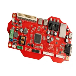
Upload your Gerber files and BOM. Our senior hardware engineers will deliver an actionable Design-For-Manufacturing (DFM) analysis report and a transparent turnkey quotation within 2 to 12 hours.