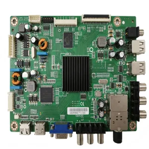
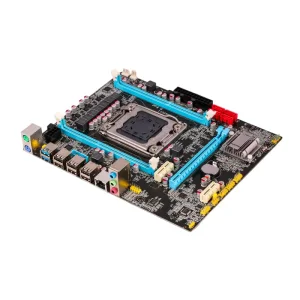
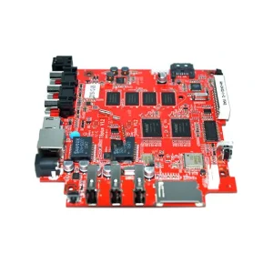
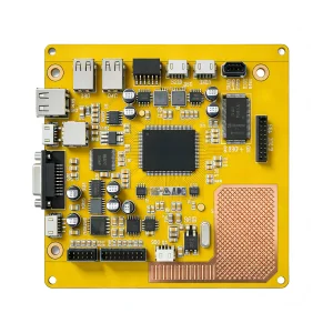
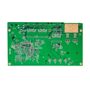
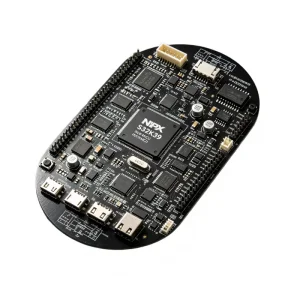
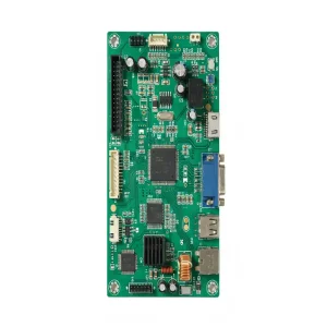
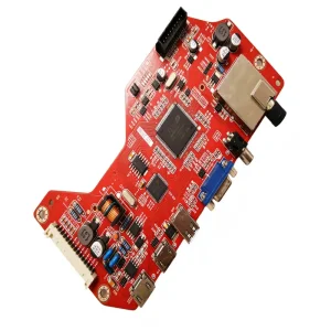
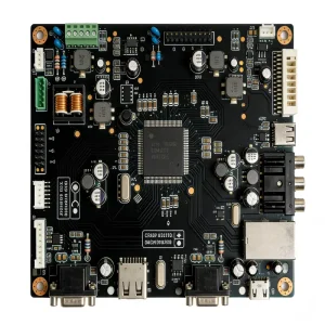
Explore our turnkey PCBA modules deployed globally across telecommunications, automotive ADAS, avionics, and medical monitoring systems.
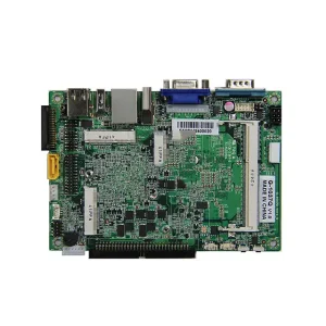
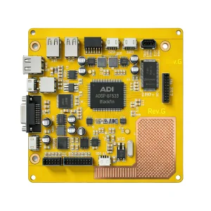
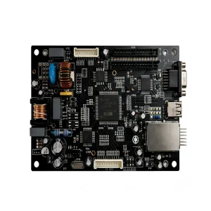
How our Shenzhen-based smart manufacturing hub bridges prototype velocity, component supply liquidity, and Tier-1 automotive and medical manufacturing rigor.
Located in Bao'an, Shenzhen—the epicenter of global electronics manufacturing—STHL operates within a 15-kilometer radius of tier-1 bare board fabricators, passives distributors, and tooling houses. This localized concentration enables us to compress multi-layer PCB turnaround to 24-48 hours and resolve unforeseen BOM component shortages in real time, delivering a structural speed advantage that offshore contract manufacturers cannot match.
Traditional EMS mega-corps often enforce massive Minimum Order Quantities (MOQs), rigid engineering change charges, and prohibitive setup costs. STHL bridges this gap by offering certified IATF 16949 (automotive) and ISO 13485 (medical) production lines with complete zero-MOQ flexibility. From pilot R&D validation to annual runs of hundreds of thousands of assemblies, quality gates remain uncompromising.
Every printed circuit board assembly moving through our factory floor is barcode-etched and tracked via our integrated Manufacturing Execution System (MES). From solder paste inspection (3D SPI) profile storage to pick-and-place nozzle telemetry, multi-zone reflow data, and automated X-ray inspection (AXI) images, our customers receive full, auditable component-level traceability for long-term field reliability.
The electronics hardware landscape is evolving rapidly under the pressures of edge AI compute, thermal limits, ultra-miniaturized packages, and strict environmental imperatives.
As smart wearables, wireless earbuds, and biometric sensors miniaturize, component real estate decreases dramatically. STHL has integrated ultra-high-speed Panasonic and Yamaha modular mounters equipped with sub-micron vision alignment systems, delivering reliable placement of 01005 and 008004 passives and fine-pitch wafer-level chip scale packages (WLCSP) down to 0.3mm ball pitch without solder bridging.
High-current EV power converters and gigabit wireless routers generate intense localized thermal loads. STHL manufactures complex Any-Layer HDI boards utilizing laser micro-vias, copper filled via-in-pad structures, heavy copper layers (up to 6oz), and metal-core substrates (IMS). These architectures rapidly evacuate heat away from critical processing dies, safeguarding continuous operational longevity.
Global environmental mandates (RoHS 3, REACH, Halogen-Free) necessitate precise metallurgical process control. STHL's 10-zone nitrogen-purged reflow ovens maintain Delta-T profiles within ±1.5°C across large boards, eliminating thermal shock on sensitive BGA silicon dies while ensuring complete intermetallic bond formation with SAC305 alloys, eliminating micro-voiding and tin whisker proliferation.
Every commercial application presents unique operating stressors. We engineer tailored PCB assembly and testing workflows to match strict environmental and functional standards.
Automotive domain controllers and LiDAR/radar sensor modules endure constant thermal cycling from -40°C to +125°C and intense mechanical vibration. Operating under strict IATF 16949 certification, STHL implements high-Tg FR-4 or polyimide laminates, automated selective conformal coating, underfill beneath ball grid arrays, and zero-defect PPM statistical process control to protect vital drive functions.
From smart infusion pumps to real-time continuous blood glucose meters, medical hardware demands exceptional accuracy and clinical reliability. Our ISO 13485 certified clean assembly bays follow stringent ESD control protocols (ANSI/ESD S20.20), rigorous optical inspection for foreign object debris (FOD), and lot-level traceability of all active and passive semiconductor devices.
Avionics systems like Electronic Flight Instrument Systems (EFIS) and Engine Indicating Crew Alerting Systems (EICAS) must operate without degradation through severe pressure drops and electromagnetic interference (EMI). STHL manufactures to IPC-A-610 Class 3 standards, executing automated X-ray analysis, specialized shield potting, and full-spectrum functional burn-in testing.
A transparent breakdown of our factory tolerances, manufacturing envelope, and equipment limits verified on active production lines in Shenzhen.
| Production & Order Flexibility | Prototype quick-turns (24-48 hrs), low-volume pilot validation, and high-volume mass production with zero Minimum Order Quantity (No MOQ). |
|---|---|
| Surface Mount Technology (SMT) | 7 fully automated SMT lines equipped with high-speed Yamaha and Panasonic mounters; 01005, 0201, micro-BGA, QFN, POP, and ultra-fine pitch ICs down to 0.3mm pitch. |
| Through-Hole Technology (THT / DIP) | 2 wave soldering and selective soldering lines; lead-free dual-wave soldering with nitrogen protection, manual insertion stations with ESD grounding. |
| Substrate Types & Materials | Standard FR-4, High-Tg FR-4 (Tg 170-180°C), Halogen-Free, Rogers RF High-Frequency, Polyimide Flexible, Rigid-Flex, Aluminum IMS, and Ceramic core boards. |
| PCB Layer Count & Tolerances | 1 to 48 layers; maximum board size 610mm × 1200mm; minimum core thickness 0.05mm; trace width/spacing down to 2.5 mil / 2.5 mil; impedance control tolerance ±5%. |
| Quality & Inspection Standards | Inline 3D Solder Paste Inspection (SPI), automated optical inspection (AOI), 3D X-Ray Inspection (AXI) for hidden BGA/QFN solder joints, First Article Inspection (FAI). |
| Testing & Value-Added Services | In-Circuit Testing (ICT), Functional Circuit Testing (FCT), Flying Probe, Thermal Environmental Cycling, IC Firmware Flashing, Conformal Coating, and Wire Harness Box Build. |
| Certified Quality Management | IATF 16949 (Automotive), ISO 13485 (Medical Devices), ISO 9001 (Quality Management), ISO 14001 (Environmental), and full RoHS/REACH compliance. |
 IATF 16949 Automotive Certified
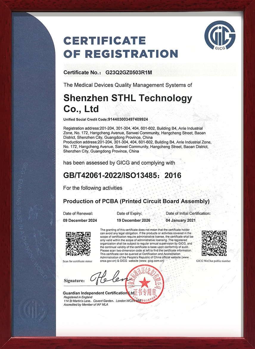 ISO 13485 Medical Devices
 ISO 9001 Quality Certified
 ISO 14001 Environmental Standard
How STHL is actively advancing manufacturing capabilities to anticipate the next decade of silicon packaging, high-speed computing, and automation.
STHL is qualifying specialized substrates and ultra-low dielectric dissipation materials (Dk < 3.0, Df < 0.002) designed for PCIe Gen 6 and 800G optical transceivers. By refining high-precision thermal compression bonding, our engineering group prepares for direct chiplet co-packaging and tight integration between RF antennas and high-speed processors.
Transitioning from post-assembly detection to proactive defect prevention, our lines are adopting machine-learning algorithmic feedback. Automated solder paste inspection systems dynamically calibrate stencil printing pressure and squeegee angles in sub-second intervals, virtually eliminating solder bridging and tombstoning before reflow occurs.
To support next-generation ultra-dense edge hardware, STHL's engineering laboratory is rolling out embedded capacitor and resistor fabrication inside inner PCB core layers. This dramatically shortens transmission path inductances, clears surface area for larger compute dies, and optimizes high-frequency power distribution networks.
From authorized silicon distribution partners to premier global original equipment manufacturers, our ecosystem guarantees authenticity, compliance, and continuity.








Engineered to exact OEM specifications, featuring high-durability substrates, comprehensive functional testing, and turnkey box build assembly.
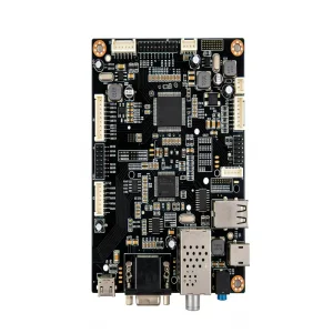
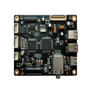
Detailed insights on intellectual property protection, component authenticity verification, DFM reviews, and international delivery timelines.
Send us your Gerber files and Bill of Materials today. Our team of 50+ process engineers will conduct an immediate Design for Manufacturing (DFM) review and deliver a complete turnkey quotation within 24 hours.