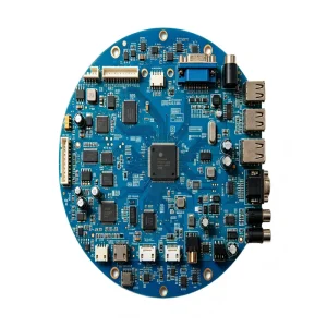
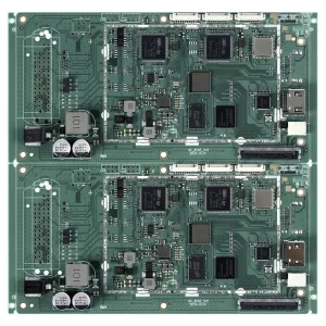
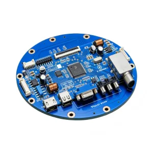
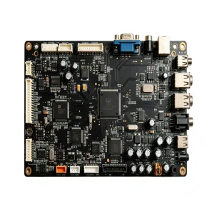
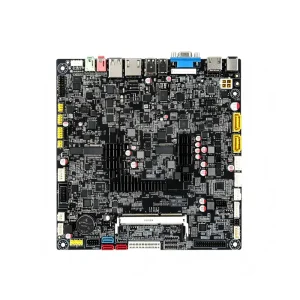
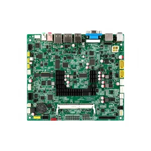
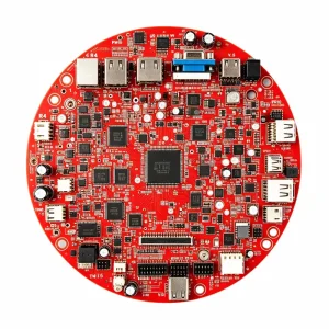
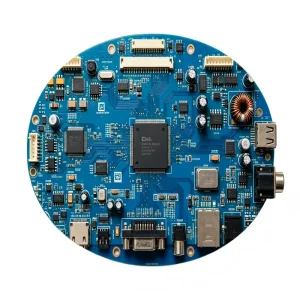
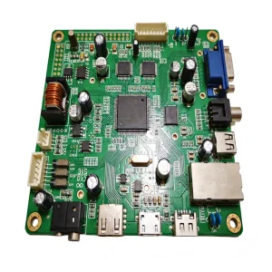
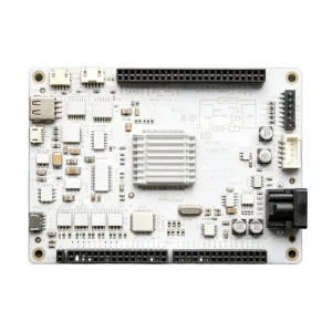
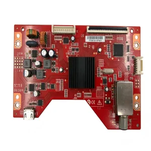
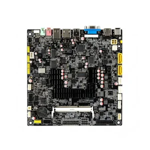
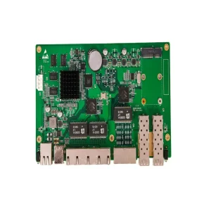
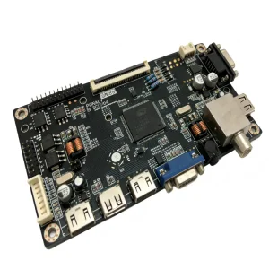
Engineered to exact IPC Class 2 and Class 3 criteria across intelligent IoT hubs, high-voltage switching, optical security platforms, and mobility architectures.
In contemporary embedded hardware development, high performance demands seamless convergence of ultra-dense micro-packaging (Surface Mount Technology) and robust, high-stress mechanical anchoring (Through-Hole Technology).
Our facility runs high-speed automated placement lines mounting down to 01005 passives and ultra-fine-pitch micro-BGAs (≤0.35mm pitch). Utilizing 3D Solder Paste Inspection (SPI) linked via feedback loops to closed-loop printers, we suppress bridging and voiding before reflow.
Where mechanical stress, high current, or connector integrity is paramount, our Dual-Wave and Nitrogen-inerted Selective Soldering processes deliver superior barrel fill (>75% per IPC-A-610 Class 3). Thermal reliefs and solder masks are dynamically optimized to eliminate cold solder defects.
Combining double-sided SMT reflow with single-pass selective through-hole soldering ensures thermal protection for sensitive ICs while securing industrial inductors, heavy terminals, and power switching MOSFETs in tight-tolerance layouts.
Shenzhen's Greater Bay Area provides an unmatched industrial cluster for electronic manufacturing services. Discover why global procurement directors rely on this ecosystem for accelerated time-to-market.
Shenzhen's industrial density places substrate fabricators, passives distributors, specialized tooling shops, and packaging specialists within a 30-kilometer radius. Prototype cycle turnaround drops from weeks to 24–48 hours, eliminating cross-border logistics friction.
Accessing 500,000+ active parts through 100+ authorized channels (Arrow, Avnet, Digi-Key, Mouser, verified Tier-1 Chinese equivalents). Our dedicated BOM engineers offer direct cross-referencing to mitigate lifecycle risks and end-of-life (EOL) bottlenecks.
We deploy proactive Value Analysis/Value Engineering (VA/VE) during the RFQ review. By proposing drop-in, pin-compatible passive and active alternatives without altering footprints, clients achieve 15%–35% direct cost reductions.
Overseas procurement teams face stringent compliance barriers. STHL pairs internationally recognized manufacturing certifications with auditable digital tracking from component reel to packaged unit.
| Standard / System | Audit Body & Scope | Target Industrial Application | Verification Protocols |
|---|---|---|---|
| IATF 16949 | Automotive Quality Management | In-Vehicle Telematics, ADAS, HUD Systems | PPAP Level 3, APQP, FMEA, CP, 100% Traceability |
| ISO 13485 | Medical Device Manufacturing | Operating Room Monitors, Diagnostic Systems | Class 100k Cleanroom, Bioburden Control, DHR Documentation |
| ISO 9001 & ISO 14001 | Comprehensive Quality & Environmental | Smart Living, Industrial Gateways, Computing | RoHS, REACH, WEEE Compliance, Closed-Loop ESD Monitoring |
| IPC-A-610 Class 2 & 3 | Workmanship Standards | Defense, Aerospace, High-Reliability Power | Automated 3D AOI, 2D/3D X-Ray Inspection, In-Circuit Testing |
How the evolution of wide-bandgap semiconductors, high-density edge devices, and localized technical deployments are redefining assembly engineering requirements.
Thermal mitigation requires copper-coin embedment and heavy-copper boards. Our mixed assembly handles compact SMT drivers while securely anchoring rugged THT current chokes and filtering assemblies without micro-cracking.
Ultra-low standby current and RF shielding demand defect-free solder fillets under micro-shields. We deploy automated conformal coating (acrylic, polyurethane, silicone) to prevent field failure in high-humidity climates.
From programming MCUs locally under strict IP custody to executing conformal coating, custom wire harnesses, mechanical fitment, and drop-shipping to end markets, we take hardware from bare silicon to fully boxed inventory.
Specialized electronics assemblies engineered for automotive HUDs, critical safety monitoring, optical computing, and robust power conversion.
In-depth technical answers addressing engineering feasibility, quality verification, IP protection, and batch delivery logistics.
Our Fuji and Yamaha automated placement systems process 01005 passives, QFN/DFN packages with 0.3mm pitch, and Ball Grid Arrays (BGA) down to 0.35mm pitch. Every fine-pitch build is validated through 3D SPI and multi-angle 3D AOI inspection.
For high-layer-count and heavy-copper PCBs (up to 12oz), we employ nitrogen-inerted selective wave soldering with dynamically adjusted preheating zones. This maintains board temperature above liquidus long enough to achieve ≥75% to 100% vertical barrel fill in accordance with IPC Class 3 specifications.
STHL procures exclusively through factory-authorized franchised distributors and direct silicon manufacturers. Incoming lots undergo rigorous incoming inspection (IQC), decapsulation testing where required, date code validation, and barcoding into our ERP/MES database for complete batch traceability.
Yes. Our lines are engineered for fast changeovers. Whether you require a 5-piece functional prototype for clinical trial validation or a 100,000-unit continuous automotive run, we offer 0 MOQ with full DFM/DFA engineering feedback provided before machine setup.
We provide full-spectrum testing: In-Circuit Testing (ICT), Flying Probe Testing for prototypes, Automated Optical Inspection (AOI), 2D/3D X-Ray Inspection for hidden solder joints/voiding analysis (<15%), Functional Testing (FCT) via custom fixtures, Burn-In/Thermal Cycling, and Dielectric Withstand testing.
We execute enforceable Non-Disclosure Agreements (NDAs) prior to receiving design data. Firmware flashing is performed via isolated local servers with encrypted hash matching, and physical access to programming cells is controlled and monitored by biometric authorization systems.