Explore precision SMT and mixed-technology assemblies manufactured with 01005 passives, ultra-fine-pitch BGAs, and automated optical validation across leading industrial applications.
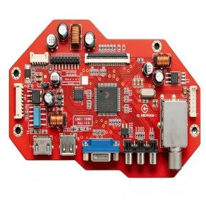
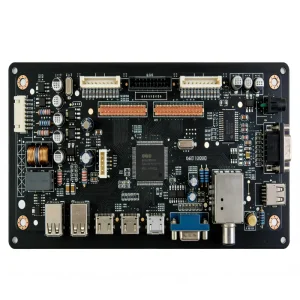
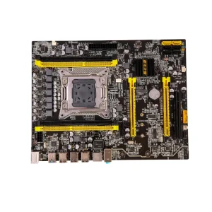

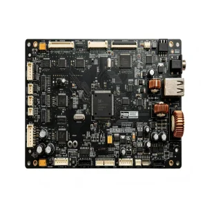
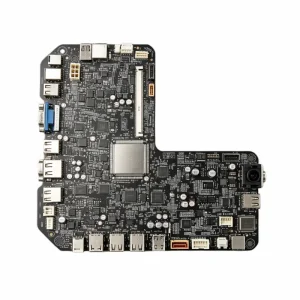

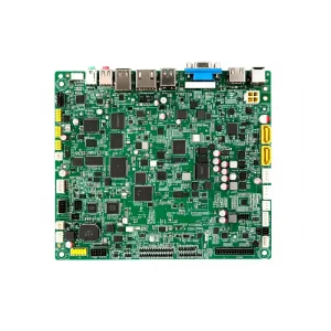
In modern electronic manufacturing services (EMS), procurement leaders face accelerating component miniaturization, acute supply chain vulnerabilities, and stringent zero-defect quality mandates across multi-tiered product lifecycles.
Procuring SMT manufacturing services extends far beyond the surface unit price. Enterprise procurement requires balancing first-pass yields (FPY > 99%), engineering rework expenses, lifecycle obsolescence handling, and end-market warranty failure rates. Minimizing hidden rework costs guarantees real bottom-line optimization.
Global semiconductor availability fluctuations require proactive BOM scrubbing and dual-sourcing strategies. Direct franchise partnerships with Arrow, Avnet, Digi-Key, and Mouser ensure full supply chain provenance, eliminating counterfeit infiltration risks through rigorous AS6081 testing protocols.
Bridging design intent and mass manufacturability early in the NPI (New Product Introduction) phase prevents cost overruns. Our technical team conducts over 80 specific automated checks across solder paste geometry, component clearance, test pad distribution, and thermal profiling.
A high-performance Surface Mount Technology line is a synchronized precision manufacturing ecosystem. Each stage features closed-loop automation, active thermal management, and 100% digital quality verification.
High-precision automatic screen printing using electroformed nano-coated stencils, coupled directly with inline 3D Solder Paste Inspection (SPI). Volumetric, height, and area deviations are flagged in real time, triggering instant automated squeegee corrections.
Dual-lane high-speed surface mounters featuring vision-guided flying cameras. Handles ultra-compact passive chips down to 01005 (0402 metric) and complex large-pitch components up to 100mm² with placement accuracy within ±0.025mm at 3-sigma.
10-to-12 zone forced convection reflow ovens running dynamic nitrogen (N2) shielding (< 100 ppm O2). Integrated vacuum reflow chambers eliminate BGA and QFN voiding, consistently keeping thermal interface void levels below 5% for high-power electronics.
Multi-frequency 3D Automated Optical Inspection (AOI) coupled with High-Resolution Automated X-ray Inspection (AXI). Validates hidden solder joints, package coplanarity, head-in-pillow (HiP) defects, and solder bridging across dense BGA/LGA packages.
| SMT Technical Metric | Production Line Capability | Quality Verification Standard |
|---|---|---|
| Min Component Package | 01005 chip passives, 0.3mm pitch CSP/BGA, QFN, POP | High-resolution optical alignment + IPC-A-610 Class 3 |
| Max Board Dimension | Dual Lane: 510mm × 460mm; Single Lane: Up to 1200mm | Dynamic PCB warp compensation & multi-clamp fixtures |
| Placement Accuracy | ±0.025 mm (±25 μm) @ Cpk ≥ 1.33 | Laser fiducial alignment & real-time vision calibration |
| Reflow Environment | 10-12 heating zones, dual-side cooling, N2 atmosphere (<100ppm) | KIC thermal profiling with 9-channel real-time loggers |
| Solder Voiding Control | Vacuum chambers reducing BGA/QFN voiding to < 5% | 3D CT Automated X-Ray Inspection (AXI) |
Tailored manufacturing controls configured to meet the rigorous regulatory, environmental, and thermal requirements across distinct electronic market sectors.
For powertrain controllers, On-Board Chargers (OBC), and ADAS modules. We enforce Automotive SPICE and PPAP Level 3 documentation, high thermal fatigue solders (SAC305/Innolot), and conformal coating for extreme temperature cycling and mechanical vibration resilience.
Applied across telemedicine gateways, MRI electronics, and surgical robotics. Characterized by rigorous device history records (DHR), biocompatible wash-free chemistries, and automated functional testing to guarantee flawless zero-failure operational continuity.
Built for industrial PLCs, smart metering, and IoT edge servers. We implement selective robotic soldering, thick-copper busbars for high current handling, automated selective conformal coating, and extended burn-in testing up to 85°C / 85% RH.
Electronic systems continue to pack higher compute density into shrinking form factors. Discover how our smart manufacturing lines evolve to tackle cutting-edge assembly hurdles.
Deploying IPC-CFX standards for synchronized machine-to-machine communication. Solder paste inspection algorithms communicate directly with printing units to offset offsets before dry runs occur, cutting solder defect rates by over 40%.
Adapting mounter head kinematics to support ultra-dense System-in-Package modules, embedded wafer-level dies, and Package-on-Package (PoP) assemblies with low-standoff underfill dispensing down to 15 μm gaps.
Pioneering bismuth-based LTS metallurgy. Lowering peak reflow temperatures from 245°C to 170°C prevents board warpage on ultra-thin flexible and HDI multi-layer substrates while slashing factory energy emissions by 25%.
Delivering high-reliability PCBA solutions backed by exhaustive process controls, institutional certifications, and round-the-clock engineering responsiveness across 90+ countries.
Every single PCB is etched with a unique 2D DataMatrix code. Our Manufacturing Execution System (MES) binds component feeder reels, placement coordinates, reflow profile telemetry, and functional test logs for up to 10 years of audit readiness.
Enforcing strict security protocols across the entire data lifecycle. Prior to receiving Gerber and BOM packages, non-disclosure agreements (NDAs) are legally ratified. Dedicated offline programming fixtures ensure microcontroller hex binaries remain encrypted.
Exporting to tier-1 OEMs across North America, Germany, the UK, Italy, and APAC. Direct logistics agreements with DHL, FedEx, and air-freight forwarders provide temperature-monitored, ESD-safe door-to-door transit with complete customs clearance assistance.
Technical and commercial answers addressing common engineering queries before initiating prototype or volume SMT turnkey projects.
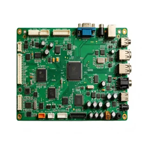
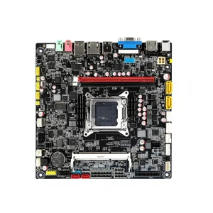
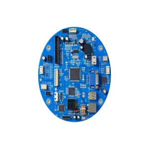
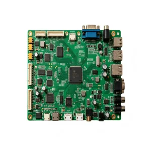
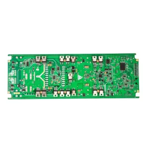
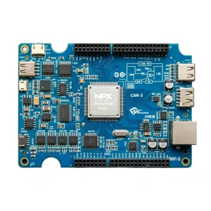
Explore additional turnkey PCBA assemblies built to stringent industrial, consumer, automotive, and RF wireless standards.

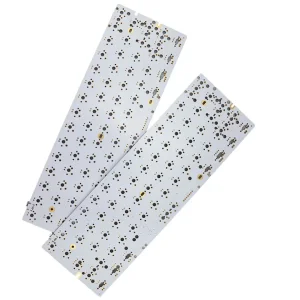
Submit your Gerber files, BOM, and assembly schematics under a binding mutual Non-Disclosure Agreement. Receive an exhaustive DFM analysis and quotation within 24 hours from our senior SMT manufacturing engineering staff.
