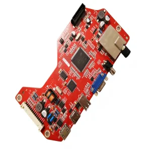
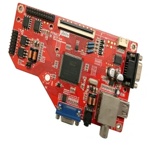
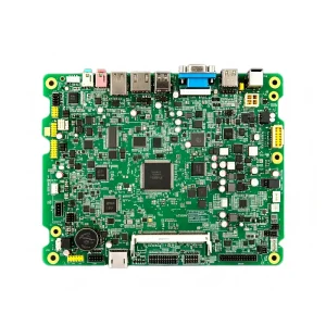
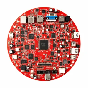
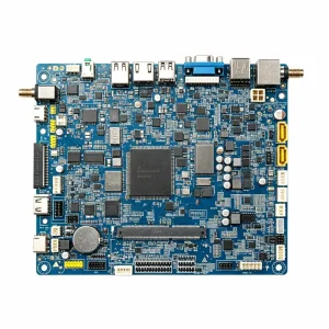
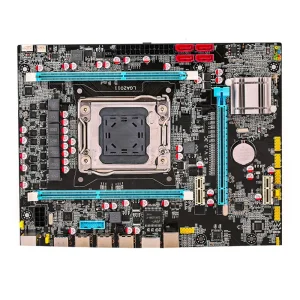
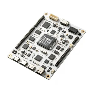
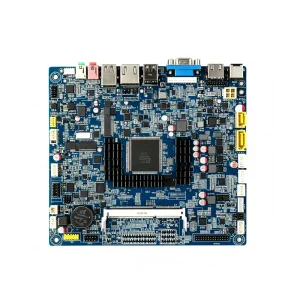
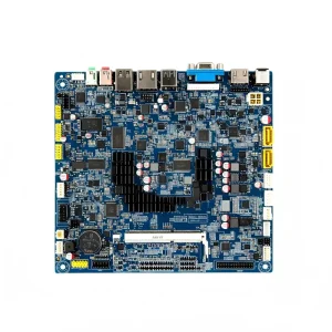
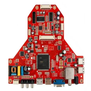
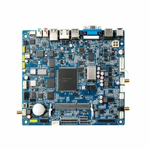
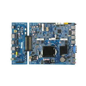
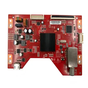
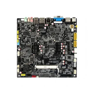
Engineered for mission-critical industrial, medical, and smart communication ecosystems. Explore the first tier of our certified turnkey contract manufacturing solutions.
Moving beyond elementary pick-and-place: How industrial-grade manufacturers achieve IPC-A-610 Class 3 compliance across micro-pitch components, high-density interconnections (HDI), and thermal-stress environments.
Surface Mount Technology (SMT) has transitioned from an automated assembly methodology into a multidimensional discipline governed by metallurgy, rheology, thermodynamics, and predictive machine vision. In contemporary high-reliability electronics—spanning automotive electronic control units (ECUs), medical implants, renewable energy inverters, and high-frequency communication modules—the barrier between acceptable functional yield and catastrophic field failure rests on micron-level process tolerances.
The root cause of approximately 65% to 75% of SMT assembly defects (such as bridging, insufficient solder, solder balls, and tombstoning) traces back directly to the solder paste deposition phase. Operating under tight engineering controls, STHL utilizes precision laser-cut electro-polished nickel stencils featuring advanced nanocoatings. The primary technical objectives during paste printing include:
| SMT Engineering Parameter | Standard Manufacturing Baseline | High-Precision / Advanced Specification |
|---|---|---|
| Minimum Passive Component Pitch | 0201 (imperial) / 0603 (metric) | 01005 (imperial) / 0402 (metric) Micro-SMD |
| Fine Pitch BGA & QFN Capability | 0.40mm Ball Pitch / 0.50mm Lead Pitch | 0.30mm Ball Pitch, Micro-BGA, PoP (Package-on-Package) |
| Component Placement Precision | ±0.035 mm (35 µm) @ Cpk ≥ 1.33 | ±0.015 mm (15 µm) @ Cpk ≥ 1.67 via Vision Alignment |
| Maximum Board Dimension | 510 mm × 460 mm | 1200 mm × 350 mm (Long-Board LED / Backplane) |
| Reflow Atmosphere & Zones | 10-Zone Air Reflow Soldering | 12-Zone Reflow with Nitrogen (N2) < 50 ppm O2 Purge |
| Inspection Verification Protocols | IPC-A-610 Class 2 Standards | IPC-A-610 Class 3 / Space & Automotive Rigorous Protocols |
A high-quality SMT assembly factory is fundamentally defined by its thermal management during reflow. Simply exceeding the 217°C liquidus threshold of lead-free SAC305 is insufficient. Complex PCBA architectures incorporating heavy ground planes alongside miniature 0201 passives face severe thermal differential challenges ($\Delta T$). STHL deploys multi-zone reflow convection ovens driven by high-purity Nitrogen ($N_2$) atmospheres that suppress oxidation and improve intermetallic compound (IMC) thickness.
Our reflow thermal engineering regulates four distinct process zones:
The geopolitical and economic reality of high-mix, high-reliability electronics manufacturing: Discover the structural efficiencies that keep the Greater Bay Area at the center of the world's hardware value chain.
Situated in Bao'an, Shenzhen, STHL is anchored in the world's most concentrated electronics cluster. Sourcing active semiconductors, passive passives, thermal substrates, and custom metal hardware occurs in hours rather than weeks. Our factory maintains established direct supply channels with authorized distributors including Mouser, Digi-Key, Arrow, Avnet, Future Electronics, STMicroelectronics, and TDK, mitigating grey-market counterfeiting while slashing lead times.
Unlike Western EMS operations that bifurcate prototype fab houses from mass production lines, Chinese factories provide true end-to-end elasticity. STHL supports zero-MOQ engineering builds that transition onto identical high-speed Fuji and Yamaha pick-and-place lines for medium-to-large runs. There is zero tooling transfer delay, zero re-qualification friction, and consistent DFM feedback from initial spin to 500,000-unit builds.
Over the past decade, premier Chinese EMS facilities have outpaced many regional Western contract manufacturers in capital reinvestment. Cleanroom environments, automated optical inspection (AOI), 3D X-ray (AXI) for BGA solder void calculation, automated conformal coating lines, and integrated ERP/MES traceability systems are standard floor assets rather than costly premium add-ons.
How artificial intelligence, extreme miniaturization, and green compliance are reshaping modern electronics contract assembly.
Traditional threshold-based optical inspection systems suffer from elevated false-call rates. Modern SMT manufacturing integrates machine-learning neural networks trained on millions of solder joint images. These algorithms accurately differentiate between benign meniscus variations and critical microscopic defects such as non-wetting opens, micro-bridging, and head-in-pillow (HiP) occurrences.
The convergence of semiconductor packaging and conventional SMT has produced System-in-Package (SiP) structures and embedded die substrates. Handling sub-0.3mm bump pitches, micro-vias, and buried passive cavities requires cleanroom class ISO 7/8 assembly environments, advanced vacuum pick arms, and sub-micron positioning accuracy.
Under IATF 16949 and ISO 13485 mandates, lot-level and board-level traceability has become non-negotiable. Individual 2D DataMatrix laser-etched bar codes on each PCB track the entire life-cycle: component reel batch numbers, solder paste lot, stencil wash cycles, exact placement nozzle identity, reflow thermal chamber logs, and functional test records.
Environmental governance demands complete elimination of hazardous halogens, alongside lower manufacturing carbon footprints. Low-temperature soldering (LTS) alloys (such as Tin-Bismuth-Silver) reduce reflow peak temperatures from 245°C down to 170°C, slashing electricity consumption while eliminating thermal warpage on delicate substrate materials.
Engineered to excel in demanding environments. How STHL's specialized manufacturing frameworks solve complex engineering challenges across strategic sectors.
Compliant with IATF 16949 frameworks. Assemblies incorporate heavy copper boards (3oz to 6oz), conformal coating against moisture ingress, and stringent thermal dissipation engineering for electric vehicle powertrain modules, smart battery chargers, and onboard driver assistance sensors. 100% automated optical inspection and thermal stress screening ensure zero field failures under severe temperature cycling (-40°C to +125°C).
Governed by ISO 13485 certified quality management systems. Applications encompass pacemaker PCBA assemblies, non-invasive patient monitors, and specialized bio-analytical sensors. Every step leverages medical-grade cleaning protocols, stringent bio-burden controls, conformal protective encapsulation, and deep component lot traceability down to the silicon die level.
Tailored for Optical Network Units (ONUs), optical transceivers, and multi-gigabit wireless access points. Our production lines maintain strict impedance control (±5%), manage controlled-depth micro-via laser drilling, and ensure micro-strip RF routing. Nitrogen reflow suppresses surface micro-corrosion, preserving signal integrity across 10Gbps+ transmission frequencies.
Covering OEM inverter systems, industrial electric forklift controllers, and electronic fence monitors. These assemblies require ruggedized through-hole technology (THT) combined with high-density SMT. Automated selective wave soldering guarantees full barrel fill (>75% per IPC Class 3) across multi-layer thick-copper boards, resisting mechanical vibrations and elevated surge currents.
Specialized high-density PCBA for wireless dimmer switches, smart home gateways, and door/window sensors. Featuring ultra-low power current draw optimization, miniature footprint layout, and integrated BLE/Zigbee/Matter antenna tuning. Automated functional testing (FCT) validates RF transmission power and receiver sensitivity on 100% of finished assemblies.
Instrumentation PCBA for real-time online water quality analyzers and low-frequency noise monitors. High-impedance analog sensor front-ends are shielded using guarded trace topologies and conformal silicone coating to eliminate parasitic leakage currents caused by ambient humidity and chemical contaminants.
A practical framework for procurement directors, VP of Hardware Engineering, and supply chain managers evaluating electronics manufacturing partners in Asia.
In modern electronic contract manufacturing, comparing piece-part quotes on a spreadsheet is the fastest path to supply chain disruption. Astute procurement organizations measure the Total Cost of Ownership (TCO), which integrates raw assembly cost, incoming component authenticity risk, engineering redesign cycles (DFM/DFA), and late delivery penalties.
High-speed telecommunications, renewable energy conversion, heavy material handling, and IoT sensor arrays manufactured to exact specifications.
Definitive engineering and procurement answers covering capabilities, quality standards, BGA soldering, and file transfer protocols.
To deliver an authoritative quotation and comprehensive Design for Manufacturability review, we require: (1) Complete Gerber files in RS-274X or ODB++ format including all copper layers, solder masks, silkscreens, and drill drawings; (2) A detailed Bill of Materials (BOM) in Excel format with explicit manufacturer part numbers (MPN), approved reference designators, package footprints, and secondary alternate part options; (3) Pick-and-Place Centroid file (X, Y coordinates, layer, and rotation angle); and (4) Assembly drawings outlining conformal coating keep-out zones, programming notes, and functional test specifications.
We control BGA solder voiding through a tripartite process: First, stencils are laser-cut with optimized round or square apertures featuring micro-cross openings to facilitate outgassing. Second, reflow profiles are tailored with Nitrogen purging to lower surface tension, maintaining peak time-above-liquidus to under 75 seconds. Third, we employ 100% 3D Automated X-ray Inspection (AXI) to measure void percentages across the inner and outer ball matrix. Voiding is strictly held below 15% (well superior to the IPC-A-610 Class 3 limit of 25%), with zero tolerance for co-planarity warping or micro-cracks.
Yes. Unlike many contract manufacturers that restrict their operations to either manual prototype labs or rigid mass lines, our 10,000+ m² facility operates 7 high-speed SMT lines and 2 THT lines. Quick-turn engineering prototypes (down to 1 to 5 boards) run on high-flexibility feeder configurations with turnarounds as fast as 24 to 48 hours following component arrival. When moving to commercial scale, the exact same machine programs, stencil apertures, and reflow recipes migrate to continuous mass production lines with zero re-engineering delay.
STHL operates under four core international quality certifications: IATF 16949 (stringent defect prevention and continuous improvement for automotive electronics), ISO 13485 (comprehensive risk management and medical device traceability), ISO 9001 (broad operational quality control), and ISO 14001 (environmental compliance and waste minimization). Our entire manufacturing floor is governed by an integrated ERP and MES system that tracks operator ID, component lot provenance, machine calibration status, and automated inspection logs per serial number.
Component authenticity is guaranteed through strict procurement hygiene. All active ICs and sensitive silicon are procured exclusively through Tier-1 authorized franchised distributors (such as Arrow, Avnet, Digi-Key, Mouser) or direct factory lines. When dealing with hard-to-find or legacy parts requested by clients, our in-house Incoming Quality Control (IQC) laboratory performs decapsulation, microscopic die marking verification, solderability testing, pin corrosion inspection, and X-ray fluorescence (XRF) lead-free RoHS verification prior to line release.
Beyond precision SMT placement, STHL functions as a comprehensive turnkey Electronic Manufacturing Services provider. Our internal post-assembly capabilities include automated selective wave soldering for mixed-technology through-hole components, automated three-axis conformal coating (acrylic, polyurethane, silicone) with UV cure, IC firmware programming and serial key injection, custom cable harness fabrication, plastic/metal enclosure box-build assembly, ultrasonic plastic welding, and complete final packaging ready for global retail or enterprise distribution.