Engineered for low signal-to-noise ratios, rugged thermal dissipation, and rigorous compliance across medical, IoT, and industrial deployments.
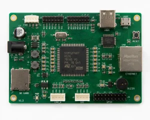
Point-of-Load Power Converter
High-efficiency DC-DC regulation
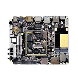
Electric Mobility Controller
High-current MOSFET drivers
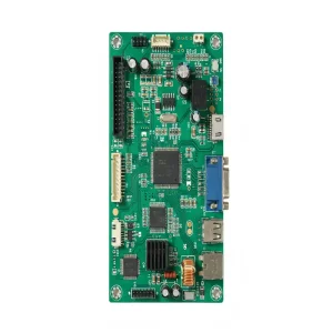
RF & Telematics GPS Receiver
Ultra-sensitive RF impedance
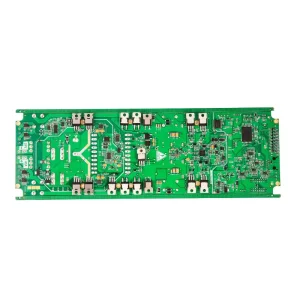
Industrial Gas Leak Detector
High-sensitivity electrochem sensing
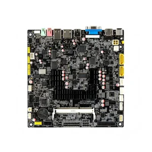
Life-Safety Carbon Monoxide Sensor
Fail-safe micro-circuitry
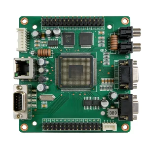
Laboratory Automation Mainboard
Multi-channel motion logic

Medical Barcode Optical Engine
Compact HDI & imaging PCBA
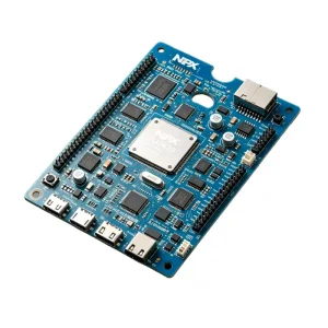
EMR Terminal Control Assembly
Hospital-grade EMC isolation
Exploring the convergence of component miniaturization, 5G/6G radio frequencies, heterogeneous semiconductor integration, and high-frequency edge compute hardware.
The electronic manufacturing services (EMS) landscape has transcended mere pick-and-place functionality. Modern engineering demands have positioned SMT Surface Mount Technology at the very nucleus of hardware innovation. As worldwide silicon architectures contract toward 3nm and 2nm nodes, the printed circuit board assembly (PCBA) has transformed into a high-frequency, thermally constrained transmission medium. The global market, valued at hundreds of billions of dollars across industrial automation, automotive electronics, and telecommunications, has shifted irreversibly from low-cost assembly paradigms to high-integrity, data-driven precision engineering.
The ubiquity of wearable medical monitors and ultra-dense IoT nodes has standardized 01005 (0402 metric) and 008004 chip passive passives. Handling these geometries requires micro-aperture electroformed stencils, sub-micron solder powder metallurgy (Type 6 and Type 7 paste), and continuous closed-loop fiducial recognition down to ±10µm alignment tolerances.
High-performance computing and edge-AI accelerators rely on wafer-level chip-scale packaging (WLCSP) and ultra-fine pitch Ball Grid Arrays (BGAs) with ball pitches below 0.35mm. Mitigating bridging, solder starvation, and inner-void formation demands programmable multizone vacuum reflow ovens and real-time automated 3D X-ray inspection (AXI).
Silicon Carbide (SiC) and Gallium Nitride (GaN) power switches generate steep thermal gradients across compact board surface areas. SMT processes must incorporate vacuum-assisted reflow soldering to minimize under-die solder voids below 5%, eliminating hot-spots and thermal runaways in automotive converters and power stage drivers.
How North American, European, and Asia-Pacific engineering enterprises evaluate Tier-1 PCBA partnerships beyond base component quotes.
In an era of volatile supply chains and geopolitical shifts, international electronics buyers—from hardware startups to Fortune 500 equipment makers—have upgraded their qualification frameworks. Sourcing decisions are no longer determined strictly by the initial BoM price; instead, Chief Procurement Officers (CPOs) and Lead Hardware Architects evaluate total lifecycle cost, intellectual property protection, and engineering responsiveness.
| Procurement Factor | Traditional EMS Vendor | STHL Smart SMT Ecosystem (Industry 4.0) |
|---|---|---|
| Design for Manufacturability (DFM) | Post-quote passive review; errors discovered during initial pilot run. | Automated pre-production DFM/DFA analysis identifying trace clearance, solder dam violations, and thermal pad discrepancies within 24 hours of RFQ. |
| Component Verification & Anti-Counterfeit | Open-market buying with intermittent visual sampling. | 100% traceable procurement via 100+ authorized global distributors, supported by incoming component testing, microscopic decapsulation, and XRF alloy analysis. |
| Prototyping to Mass Production Scaling | Prototypes built on manual lines; full re-qualification needed for mass SMT. | Unified production equipment across all batch sizes. High-speed dual-beam placers accommodate rapid NPIs with zero minimum order quantity (No MOQ) requirements. |
| Data Traceability | Batch-level paper logs; disconnected post-assembly records. | MES-driven individual board serial tracking (UID): solder paste thickness, reflow temperature curves, AOI/AXI optical captures, and functional testing logs tied to ERP. |
Leveraging deep industrial agglomeration, algorithmic manufacturing systems, and turnkey hardware turnaround.
Located in the heart of Shenzhen's Bao'an District, our manufacturing operations sit within minutes of global silicon stockists, PCB substrate panelizers, high-precision metal stamping facilities, and plastic injection tooling factories. This hyper-dense ecosystem compresses material staging windows from weeks down to hours.
From automatic solder paste printers with SPI (Solder Paste Inspection) feedback loops to high-speed multi-head pick-and-place lines, our shop floor is synchronized via modern MES architecture. Every component lot is dynamically monitored to prevent line starvation, placement drift, or reel cross-contamination.
Our operations comply with stringent global benchmarks: IATF 16949 for zero-defect automotive electronics, ISO 13485 for medical device manufacturing, ISO 9001 for end-to-end quality assurance, and ISO 14001 for sustainable, RoHS/REACH compliant manufacturing.
From extreme thermal cycles in industrial plants to hospital bedside diagnostics, our surface mount assemblies deliver uninterrupted reliability.
Class III-ready SMT processes for medical telemetry, analytical lab balances, and bedside ventilators. Features cleanroom conformal coating, non-conductive staking, and 100% boundary scan testing ensuring complete patient isolation and electrical compliance.
Built under IATF 16949 control plans for BMS battery monitoring, traction inverters, and onboard telematics. Board builds integrate high-reliability lead-free alloys (SAC305/SN100C) and automated optical inspection for vibration-proof solder fillets.
Long-life edge gateways, toxic gas monitors, and vibration analyzers deployed in harsh field enclosures. Assemblies resist broad temperature extremes (-40°C to +125°C) and feature potting and polyurethane conformal barriers against sulfur corrosion.
Multilayer FR-4 and Rogers hybrid PCB stack-ups for high-bandwidth transceivers and telecom repeaters. Precision impedance matching (controlled dielectric constants) paired with sub-millimeter component placement guarantees signal integrity up to microwave bands.
A rigorous examination of solder joint metallurgy, intermetallic layer formation, and thermo-mechanical reliability.
At the microscopic level, an SMT solder joint is not merely a mechanical anchor; it is a complex metallurgical interface. High-reliability electronics assembly demands complete control over intermetallic compound (IMC) thickness, specifically the Cu6Sn5 (eta-phase) and Cu3Sn (epsilon-phase) interfaces formed during liquidus-to-solidus transitions.
Our surface mount lines utilize high-definition laser-cut stencils with nanocoating surface treatments. By tuning area ratios (AR > 0.66) and employing enclosed squeegee systems, we maintain paste transfer efficiency above 95% on fine-pitch 0.4mm CSPs, mitigating cold joints and bridging defects.
Ten-zone forced-convection ovens equipped with nitrogen (N2) blanketing reduce oxygen concentration below 500 ppm. This suppresses tin oxidation, enhances wetting velocities, and controls the Time Above Liquidus (TAL) within a narrow 45–60s window to keep the intermetallic boundary between 1.5µm and 3.0µm.
A defect eliminated before wave or reflow saves 10x downstream testing costs. We deploy an inline triple-check regimen: 3D SPI measures volumetric paste deposit before chip placement; dual-wavelength 3D AOI detects component coplanarity and tombstoning; and off-axis 3D AXI computes BGA voiding ratios.
Key technical and commercial inquiries answered by our senior engineering, sourcing, and quality assurance personnel.
STHL maintains a flexible zero-MOQ policy. We assemble quick-turn engineering prototypes (from 1 to 50 boards) within 24 to 72 hours following DFM approval and component kitting. Full-scale production lots scale seamlessly across our 7 automated SMT lines without requalification barriers.
Prior to reviewing Gerber, ODB++, or BoM files, we execute standard non-disclosure agreements (NDA). Files reside on an encrypted, access-segregated internal engineering network. In addition, firmware flashing protocols take place over secure off-network automated stations to eliminate firmware exfiltration risks.
To deliver an itemized quotation within 24 hours, our engineering staff requires: (1) Gerber RS-274X or ODB++ files, (2) an itemized Bill of Materials (BOM) in Excel with manufacturer part numbers (MPN), (3) XY Pick-and-Place (Centroid) data, and (4) specific test criteria or assembly drawings.
Our dedicated procurement engineering team conducts proactive life-cycle risk assessments upon BOM ingestion. When end-of-life (EOL) or allocations emerge, we formulate drop-in pin-compatible alternate proposals backed by complete datasheets, pin-out comparisons, and engineering verification samples.
Beyond surface mount (SMT) and through-hole (THT) insertion, STHL provides automated selective conformal coating, silicone/epoxy potting, ultrasonic plastic welding, custom wire harness integration, full-system box build assembly, and custom packaging for turnkey shelf-ready delivery.
Every PCBA undergoes In-Circuit Testing (ICT) or Flying Probe testing to catch component deviations and open/shorts, supplemented by Automated 3D Optical Inspection (AOI) and X-ray analysis for fine-pitch BGAs. We build custom functional testing (FCT) test jigs simulating active operating environments.
Explore additional turnkey circuit card assemblies manufactured to international IPC-A-610 Class 2 and Class 3 electronic standards.
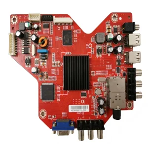
CCTV Security Monitor PCBA
Low-noise visual processing
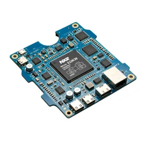
Clinical Anesthesia Controller
Class-III medical redundancy

Heavy Vehicle Forklift Controller
Rugged high-voltage PCBA
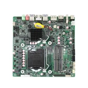
Biological Laboratory Analyzer
Sub-picoamp precision measurement
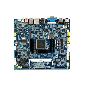
Optical Telecom Transceiver
Multi-gigabit high-speed RF
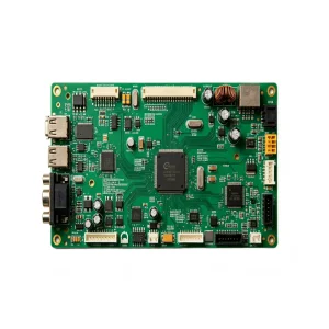
Bluetooth Audio Headset PCBA
Ultra-compact rigid-flex form
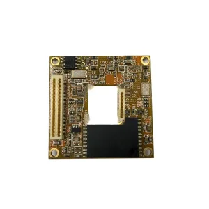
Enterprise VoIP Communications
Integrated DSP voice processing
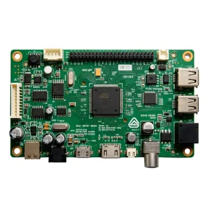
Data Center Load Balancer
High-throughput compute card
