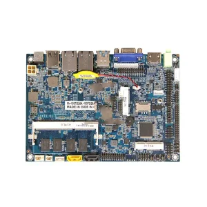
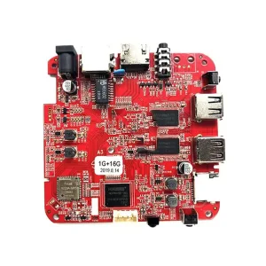
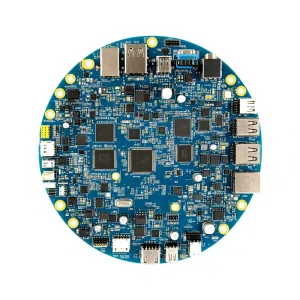
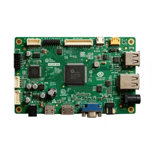
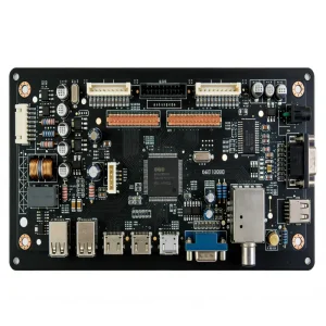
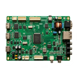
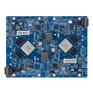
Explore production-grade turnkey assembly deployed across optical, network, security, and industrial IoT ecosystems worldwide.
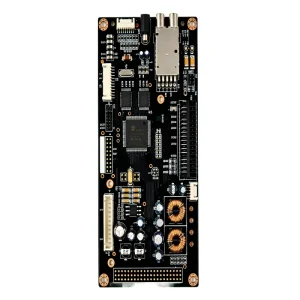
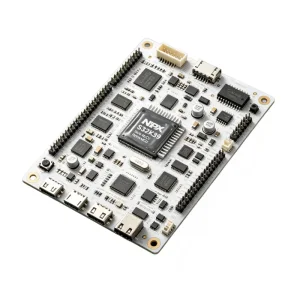
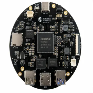
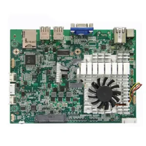
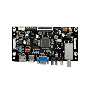
Strategic analysis of multinational supply chain mitigation, multi-sourcing agility, and total cost of ownership (TCO) optimization.
Global hardware vendors demand agile component supply matrices. STHL actively resolves long lead times via our vetted network of 100+ authorized global distributors, maintaining second-source lifecycle contingency mapping for critical semiconductor components.
Enterprise procurement requires verifiable digital footprints. Every PCBA manufactured at STHL is tracked from raw substrate through pick-and-place, reflow thermal profiles, and AOI/X-ray metrics via serialized QR/barcodes bound to unified MES systems.
Eliminating minimum order quantity (No MOQ) barriers allows Tier-1 R&D laboratories to run rapid NPI (New Product Introduction) cycles on the exact high-precision surface-mount lines later dedicated to multi-million unit commercial rollouts.
Real-time manufacturing readiness backed by modern smart manufacturing automation and 20 years of sector-specific engineering discipline.
Turnkey electronic contract manufacturing calibrated to withstand severe operating environments, strict regulatory thresholds, and long product lifecycles.
IATF 16949-audited PCBA production ensuring zero-defect standards for EV charging piles, advanced driver assist units, BMS controllers, and vehicle telematics.
ISO 13485-certified assembly lines executing precision layout, cleanroom conformal coating, and strict component genealogy for in-vitro diagnostics and monitoring sensors.
Heavy-copper PCB assembly, robust THT soldering, and automated selective soldering built to resist thermal shocks, vibration, and continuous electromagnetic interference in PLCs.
Micro-fine pitch component placement down to 01005 passives and ultra-dense 0.3mm BGA chips, integrated with high-frequency RF impedance simulation and 5G base station protocols.
Forward-thinking investments in automated intelligence, material science, and high-frequency HDI circuit manufacturing.
Integration of deep-learning algorithms into 3D AOI and 3D AXI (Automated X-ray Inspection) systems to completely eliminate solder bridging false positives and detect micro-voids in hidden bottom-termination BGA balls below 10% void area tolerances.
Expanding direct-bond copper (DBC), ceramic aluminum-nitride substrates, and ultra-thin flexible polyimide circuits for extreme power conversion efficiencies demanded by GaN/SiC electric automotive powertrains and industrial energy storage.
Full implementation of Industry 4.0 smart factory connectivity, synchronizing solder paste printer pressure parameters, component mounter speeds, and multi-zone reflow oven thermography automatically via edge IoT sensors.
Seamless international trade navigation, RoHS/REACH compliance, and intellectual property fortifications.
Strict non-disclosure agreements (NDA) legally executed before any engineering evaluation or RFQ processing. Design databases, schematics, and proprietary firmware are isolated inside air-gapped localized storage networks accessible only by cleared engineers.
Every PCBA batch conforms strictly to international green directives including RoHS 3 (EU 2015/863), REACH compliance, UL94V-0 flammability certifications, CE marks, and FCC emission limits, supported by full laboratory material test sheets upon request.
Direct communication bridges between Western client R&D labs and STHL front-line manufacturing engineers eliminate cultural or technical ambiguities, accelerating DFM/DFA feedback iterations within 24 hours of Gerber upload.
Comprehensive technical clarifications for hardware designers, procurement officers, and quality control directors.
STHL maintains direct partnerships and verified supply agreements with original component manufacturers (OCM) and tier-1 authorized distributors such as Digi-Key, Mouser, Arrow, Avnet, and Element14. Incoming parts undergo rigorous inbound inspection, verification of lot date codes, packaging integrity checks, and micro-imaging validation where required.
Prior to manufacturing launch, our 50+ member engineering team executes automated and manual DFM/DFA checks against your Gerber layers and BOM. We inspect trace-to-copper spacing, test pad exposure, thermal relief geometry on ground planes, component body clearances, and solder paste aperture thickness to prevent solder bridges, tombstones, and voids.
Yes. Beyond SMT and THT assembly, we operate 2 dedicated functional test lines and 2 full system assembly lines. We build customized functional testing (FCT) jigs, perform In-Circuit Testing (ICT), conduct flying probe tests, burn-in thermal cycling, and execute complete mechanical enclosure assembly, wire harnesses, conformal coating, and final retail packaging.
Our 10,000+ m² facility is architected for maximum line agility. Dedicated SMT lines are assigned strictly to quick-turn NPI prototypes, capable of 24- to 48-hour turnarounds once materials are staged. Because our prototyping runs on the exact same high-precision Siemens and Yamaha placement machines as our mass lines, transitioning to volume runs requires zero re-tooling.
Custom electronics manufacturing applications across EV charging piles, environmental monitoring, audio processors, and industrial automation.