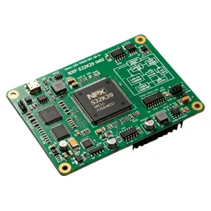
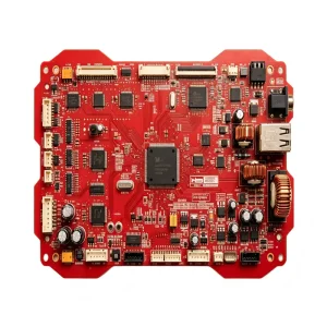
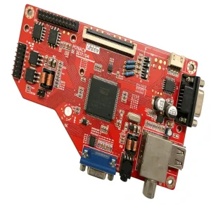
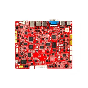
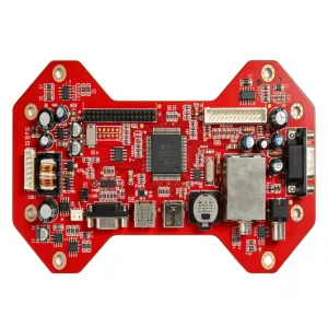
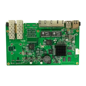
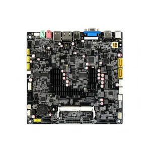
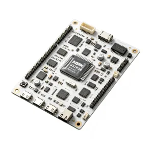
Explore our mission-critical electronic assemblies manufactured via high-speed, 01005-capable automated surface mount production lines with zero-defect quality benchmarks.
In modern electronics manufacturing, the Surface Mount Line (SMT Line) acts as the quintessential nervous system of hardware industrialization. Over the past decade, worldwide demand for hyper-dense, multi-layered Printed Circuit Board Assemblies (PCBAs) has surged exponentially, driven by electrification in the automotive sector, heterogeneous semiconductor packaging, hyperscale cloud computing, and next-generation biomedical devices. High-quality surface mount line services and advanced contract manufacturing facilities are no longer merely assembly vendors; they are critical R&D extension hubs operating under strict Design for Manufacturability (DFM) and Design for Excellence (DFX) methodologies.
As microelectronics shift from conventional SMD passives to sub-millimeter components (such as 03015 and 01005 metrics) alongside wafer-level chip-scale packages (WLCSP) and ultra-fine pitch Ball Grid Arrays (BGA with pitch < 0.35mm), traditional mechanical placement methods are entirely obsolete. The modern surface mount factory integrates closed-loop solder paste printing, high-speed multi-gantry modular placement equipment capable of placing up to 100,000 components per hour (CPH), multi-zone nitrogen reflow ovens with dynamic thermal profiling, and 3D automated optical inspection (3D AOI / 3D SPI). Global OEMs navigating supply volatility require certified partners backed by IATF 16949, ISO 13485, and robust MES digital tracing to safeguard against board warping, micro-voiding, solder bridging, and component degradation.
How intelligent automation, digital twins, and advanced metallurgical control are transforming factory lines into agile, self-correcting manufacturing ecosystems.
Integration of 3D Solder Paste Inspection (SPI) directly communicating with intelligent stencil printers via CFX/IPC-HERMES protocols. Automatic stencil alignment, pressure adjustments, and proactive wipe cycles mitigate 70%+ of reflow soldering defects before component mounting occurs.
System-in-Package (SiP) and flexible circuit manufacturing demand cleanroom SMT environments with micro-dispensing, vacuum reflow soldering, and flux-less formic acid heating to ensure under-die void rates drop below 5% for safety-critical automotive compute units.
Complete digitization from incoming reel scanning to single-board serialization. Micro-QR laser markings map exact solder batch, nozzle pressure, feeder reel ID, and reflow peak temperatures for full lifecycle recall prevention and aerospace compliance.
Tailored SMT assembly configurations addressing distinct thermal, mechanical, and electro-chemical stressors across specialized industrial segments.
VCU, On-Board Charging (OBC), and Battery Management Systems (BMS) subject to high thermal cycling (-40°C to 125°C). Utilizing heavy-copper PCB fabrication, vacuum vapor-phase soldering, and automated robotic selective conformal coating to eliminate dendrite growth.
Precision implantable devices including pacemakers, smart hearing aids, and OEM drug delivery mechanisms. Fabricated inside certified ISO 13485 dust-free environments utilizing bio-compatible soldering alloys, ionic contamination testing, and 100% 3D X-ray inspection.
DIN Rail industrial power supplies, high-voltage DC-DC converters, and multi-sensor water leak monitoring systems. Built with thick copper layers, optimized thermal vias, and potted assemblies to endure severe electromagnetic interference (EMI) and physical vibration.
VoIP hardware, high-frequency smart security modules, and edge AI gateways. Incorporating fine-pitch BGA mounting, controlled dielectric PCB fabrication (Rogers/High-Tg FR4), and rigorous RF shielding integration to maximize signal integrity and prevent packet loss.
How tier-1 SMT manufacturing facilities bridge the gap between initial prototyping and massive multi-million unit commercialization.
Every CAD/Gerber dataset passes through automated DFM rules evaluating solder bridge risks, pad aspect ratios, component spacing, and fiducial mark placement. Identifying pad geometry mismatches prior to stencil fabrication saves 30%+ in potential re-spin costs and eliminates assembly line halts.
Integrated with tier-1 authorized distributors and global component broker databases. Proactive lifecycle analysis flags End-of-Life (EOL), Not-Recommended-for-New-Designs (NRND), and lengthy lead-time ICs, providing drop-in pin-compatible alternatives to prevent manufacturing bottlenecks.
From In-Circuit Testing (ICT) and Flying Probe testing to In-System Programming (ISP) and Functional Circuit Testing (FCT). Assemblies endure burn-in thermal chambers, drop simulation, and salt-mist corrosion testing to guarantee flawless field performance across critical duty cycles.
In-depth answers to the core questions asked by hardware engineering directors, quality auditors, and supply chain managers.
Our advanced Yamaha and Panasonic high-speed SMT lines comfortably mount micro passive components down to 01005 (0402 metric) and 03015 sizes, with placement accuracy tolerances within ±0.03mm (3 sigma). We also specialize in ultra-fine-pitch BGAs (down to 0.3mm pitch) and 0.4mm pitch QFN packages.
We employ nitrogen-purged 10-zone reflow ovens coupled with 3D Solder Paste Inspection (SPI) to ensure consistent paste height and volume. Post-reflow, 100% of BGA, QFN, and critical IC components undergo automated 3D X-Ray Inspection (AXI) to verify voiding levels remain below 15% (well surpassing the IPC Class 3 threshold of 25%).
Our factories operate under rigorous international quality architectures: IATF 16949 (Automotive), ISO 13485 (Medical Devices), ISO 9001 (Quality Management), and ISO 14001 (Environmental Standards). All assembly technicians and inspection operators are certified to IPC-A-610 Class 2 and Class 3 workmanship criteria.
Yes. We enforce a strictly zero-MOQ policy. We operate dedicated Quick-Turn SMT prototyping lines capable of delivering 24-to-48-hour turnarounds on initial sample batches, seamlessly transferring identical stencil apertures and feeder profiles to high-speed mass production lines without requiring engineering re-qualification.
Explore our specialized automotive controllers, medical lifesavers, power converters, and safety-critical wireless hardware manufactured on our high-precision surface mount lines.