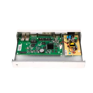
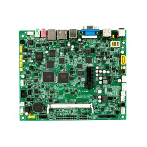
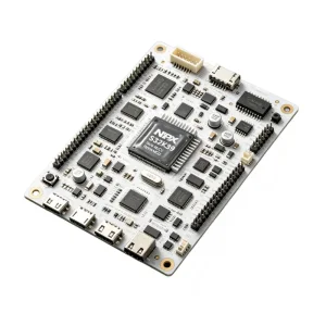
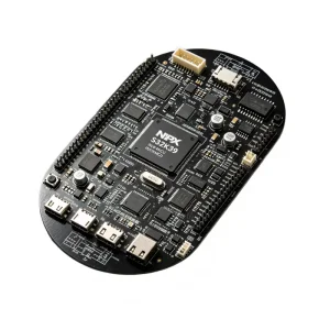
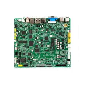
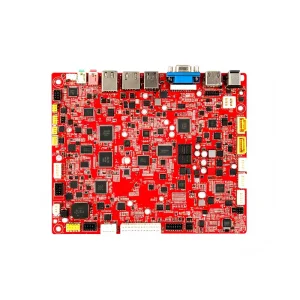
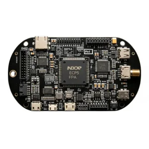
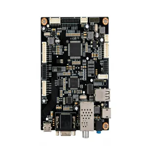
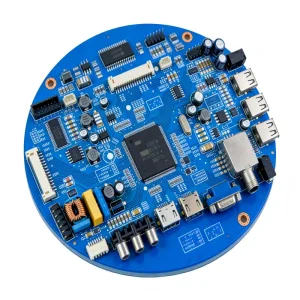
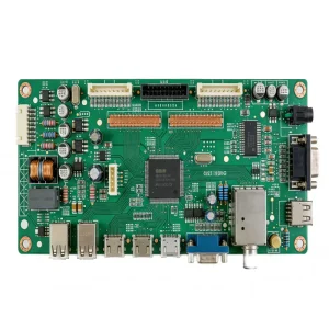
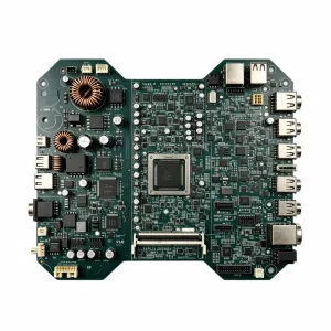
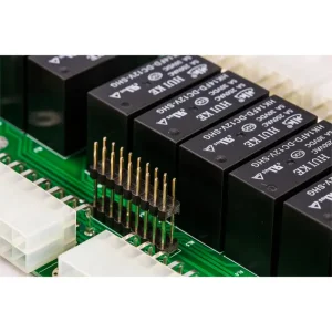
Explore our active OEM production builds spanning optical monitoring, programmable dynamic power, fail-safe perimeter defense, and automated industrial crane controls engineered to IPC-A-610 Class 3 standards.
Deciphering the paradigm shift toward micro-miniaturization, heterogeneous chip packaging, and supply-chain diversification in modern electronics manufacturing.
The contemporary electronics ecosystem is dominated by higher processing densities, narrower signal path traces, and dense multi-layer substrate architectures. Surface Mount Technology (SMT) has transitioned beyond legacy 0402 and 0201 metrics into ultra-dense 01005 (0402 metric) and 03015 micro-passives.
Original Equipment Manufacturers (OEMs) worldwide require manufacturing partners that deliver the agility of rapid prototyping alongside certified, scalable volume production lines. Mitigating geopolitical exposure requires localized engineering support coupled with end-to-end component traceability.
Electronics deployed in smart energy storage, high-vibration heavy industrial machinery, and automotive drivetrains face severe thermal shocks, humidity, and corrosive particulate exposure. Assembly standards must transcend generic commercial guidelines.
A comprehensive engineering baseline designed for hardware developers, systems architects, and technical sourcing teams requiring empirical tolerance specifications.
| Assembly Parameter | Standard Commercial Specification | Advanced OEM Class 3 Specification (STHL Production) |
|---|---|---|
| Minimum Passive Placement | 0402 Imperial (1005 Metric) | 01005 Imperial (0402 Metric) & 03015 Ultra-Dense Micro-Components |
| Fine-Pitch IC & BGA Ball Pitch | 0.50 mm (19.7 mil) Pitch | 0.25 mm (9.8 mil) Pitch, Micro-BGA, PoP (Package-on-Package), WLCSP |
| PCB Dimensional Handling (Max/Min) | 50 mm × 50 mm up to 450 mm × 400 mm | 50 mm × 50 mm up to 1200 mm × 600 mm (Long-Board LED / Backplane Panels) |
| Substrate Compatibility | Standard Rigid FR-4 (Tg 130°C - 150°C) | High-Tg FR-4 (170°C+), Rigid-Flex, Polyimide Flex, Metal Core (Al/Cu), Rogers RF, Ceramic |
| Reflow Atmosphere & Soldering | Standard Forced Air Convection (Air) | 10-Zone Nitrogen (N2) Atmosphere Reflow, Dual-Wave Soldering, Selective Solder Fountains |
| Optical & Structural Inspection | Sampled Post-Reflow 2D AOI | In-line 3D Solder Paste Inspection (SPI), Dual-Sided 3D AOI, High-Resolution 2D/3D X-Ray (AXI) |
| Traceability & MES Interconnection | Batch/Lot Level Tracking | Component-Level UID Serialization, Barcode 2D Datamatrix, Solder Lot Traceability |
| Testing & Screening Protocols | Basic Continuity & Power-On Check | Flying Probe, Bed-of-Nails ICT, Functional Testing (FCT), Boundary Scan, Burn-in Environmental Chambers |
Navigating strict regional and vertical certifications to guarantee zero border delays, seamless customs clearance, and verified device safety across North America, Europe, and Asia-Pacific.
Engineered for mission-critical automotive subsystems including powertrain controllers, advanced driver-assistance systems (ADAS), infotainment consoles, and battery management systems (BMS). Our lines execute strict APQP, PPAP Level 3 documentation, FMEA analysis, and error-proofing (Poka-Yoke) assembly methodologies.
Full process validation for Class II and Class III life-critical medical devices. From smart glucose meters to surgical biochemical analyzers, we uphold rigorous ESD Class 100,000 dust-free cleanroom environments, biocompatible materials verification, and long-term Device History Record (DHR) archiving up to 15 years.
Sustained operational consistency anchored by ISO 9001 quality management and ISO 14001 environmental sustainability. Complete hazardous substance control adhering to RoHS 3 Directive (EU) 2015/863, REACH (EC 1907/2006), and conflict-free mineral sourcing policies certified across all bill-of-materials layers.
From distributed solar infrastructure to industrial robotics and clinical diagnostics, discover how our custom turnkey PCBA models perform in real-world operating environments.
Solar inverters, maximum power point tracking (MPPT) units, and string monitoring systems endure continuous extreme thermal cycling and high transient voltages. We build heavy-copper (3oz - 6oz) power boards integrated with galvanic isolation, custom inductive coils, and heat-sink thermal bonding designed for 25-year service life.
Heavy cranes and automated port logistics machinery operate under relentless mechanical vibration, wide harmonic distortion, and electromagnetic interference (EMI). Our PCBA designs incorporate reinforced THT mounting anchors, anti-vibration staking silicone, and comprehensive potting solutions tested against MIL-STD-810 shock curves.
Gas leak detectors, electronic fence sensors, and enterprise surveillance camera PCBA modules require low-noise RF signal preservation and ultra-low quiescent current standby modes. We deliver impedance-controlled RF circuit manufacturing (50Ω / 100Ω differential) matched with automated high-speed firmware flashing and RF calibration.
A strategic technological trajectory illustrating how STHL invests in next-generation microelectronics, automated manufacturing intelligence, and substrate innovations.
Integration of real-time computer vision models across SPI and AOI stations. Solder paste volume variations dynamically feed back to adjust stencil printer blade pressure and reflow oven zone temperature profiles in sub-second intervals.
Migrating discrete passive arrays and semiconductor dies directly into internal PCB core cavities. This drastically shrinks outer package silhouettes while mitigating parasitic inductance for multi-gigahertz edge computing hardware.
Refining laser direct imaging (LDI) for sub-25μm trace/space geometries on PTFE and liquid crystal polymer (LCP) materials, delivering stable high-frequency dielectric constant performance for satellite communications and 6G infrastructure.
Transitioning toward bio-resin dielectric substrates and low-temperature bismuth-tin (BiSn) solders that lower reflow thermal budgets by 40°C, drastically curbing production carbon footprints while maintaining industrial shear strength.
Clear, verified guidance addressing technical constraints, quality verifications, and contractual assurances for global procurement professionals.
Our dedicated team of 50+ engineers executes a multi-point Design for Manufacturability (DFM) and Design for Assembly (DFA) audit. We inspect via-in-pad geometry, thermal relief pad ratios, solder mask slivers, component clearance to board edge, and centroid accuracy. Resolving design anomalies prior to tooling eliminates copper redesign charges and guarantees first-pass yield above 99%.
We source directly from original component manufacturers (OCM) and authorized global distributors (Arrow, Avnet, Digi-Key, Mouser). For broker-sourced legacy parts, materials pass through incoming visual inspection, decapsulation, XRF elemental metallurgy checks, pin-to-pin electrical parameter screening, and solderability tests under our rigorous IATF 16949 / ISO 9001 certified QA system.
Yes. We enforce a strict No Minimum Order Quantity (No MOQ) policy. Whether your engineering team requires 5 prototype boards for preliminary EMC testing or 500,000 units for global commercial rollout, your project is produced on identical high-precision SMT lines, guaranteeing seamless transition from NPI (New Product Introduction) to full mass production.
Visual inspection is physically impossible for bottom-terminated components. We employ automated transmission X-Ray Inspection (AXI) to analyze solder ball coplanarity, bridge formation, and void percentages under BGAs. In accordance with IPC Class 3 standards, BGA voiding is maintained strictly under 15% (and under 10% upon customer engineering specification).
Our 10,000+ m² facility delivers true end-to-end turnkey Electronic Manufacturing Services (EMS): custom PCB layout, automated conformal coating, firmware flashing, custom wire harness integration, ultrasonic plastic welding, box-build mechanical assembly, and retail-ready ESD packaging shipped worldwide to 90+ countries.
We execute legally binding Non-Disclosure Agreements (NDAs) prior to receiving Gerber or BOM files. Firmware flashing is performed through isolated, air-gapped programming fixtures with restricted technician access. All IP files are stored on enterprise-encrypted on-premise servers shielded from unauthorized external network access.
A second collection of production-proven assemblies engineered across certified medical diagnostics, automotive infotainment, and smart IoT platforms.
Send your Gerber files, Bill of Materials (BOM), and assembly drawings. Our senior engineering staff will furnish a comprehensive DFM evaluation, component availability report, and transparent cost proposal within 24 hours.