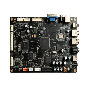
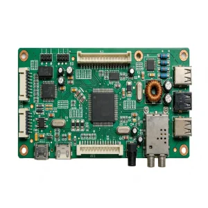
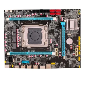
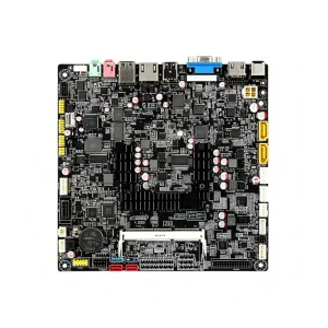
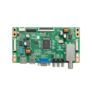
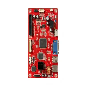
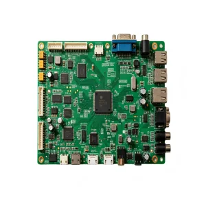
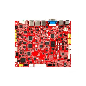
Direct engineering snapshots from our high-precision SMT and THT production lines, demonstrating capability across aerospace, telecommunications, and industrial automation.
How microelectronics miniaturization, high-speed signals, and thermal dynamics are revolutionizing modern OEM printed circuit board manufacturing.
Traditional through-hole interconnects are no longer sufficient for 0.4mm pitch ball grid arrays (BGAs) and system-in-package (SiP) modules. Modern OEM advanced circuit manufacturers utilize laser-drilled blind and buried microvias (1+N+1 to 4+N+4 architectures) to achieve interconnect densities unattainable with conventional mechanical drills.
As operating frequencies in edge telecommunications and automotive radar expand from 5.8GHz to 77GHz, standard FR-4 dielectric losses become intolerable. Advanced circuit factories balance cost and signal integrity by engineering hybrid stackups utilizing high-frequency substrates alongside standard core laminates.
Modern power conversion modules, aerospace flight display computing units, and industrial motor drives require massive thermal dissipation. Advanced circuit OEM factories leverage heavy copper foils (up to 10oz) combined with embedded copper coins and ceramic-filled prepregs to pull junction temperatures safely away from silicon cores.
Why Tier-1 hardware enterprises, medical device developers, and automotive disruptors maintain high-volume advanced PCBA partnerships in Shenzhen, China.
Shenzhen represents the geographic nucleus of passive, discrete, and active semiconductor trade. While Western manufacturing partners face 12 to 24-week delivery horizons for complex BOMs, STHL leverages relationships with 100+ authorized distributors (including Mouser, DigiKey, Arrow, Avnet, and domestic franchised suppliers) to source over 500,000 active part numbers, eliminating production starvation.
Integrated turnkey fabrication eliminates the costly handoff delays between bare-board laminators and assembly houses. At STHL's 10,000+ m² Bao'an facility, engineering questions (EQs) are resolved in under 2 hours. DFM/DFA checks occur concurrently with raw substrate procurement, compressing typical 6-week prototyping windows down to 5 to 7 operational days.
Western procurement managers often worry about counterfeit components and latent defects. STHL negates these risks through multi-stage quality gates: 100% incoming component XRF and electrical verification, automated solder paste inspection (SPI), dual-lane 3D automated optical inspection (AOI), 3D transmission X-ray (AXI) for BGA void verification, and in-circuit functional testing.
How high-reliability OEMs engineer printed circuit assemblies to survive severe thermal shock, high vibration, electromagnetic interference, and stringent regulatory environments.
Certified under IATF 16949, our manufacturing lines produce mission-critical Electronic Parking Brake (EPB) controls, in-vehicle telematics, and battery management systems (BMS). Using high-Tg FR-4 (Tg ≥ 170°C), conformal silicone coating, and underfill for high-vibration resilience, these assemblies survive ISO 16750 thermal cycling from -40°C to +125°C.
Under an ISO 13485 quality management infrastructure, we assemble biomedical sensing boards, bedside monitoring devices, and ultrasonic imaging hardware. Manufacturing controls mandate IPC-A-610 Class 3 soldering tolerances, zero ionic contamination via automated deionized wash systems, and complete MES work-order trace histories down to specific silicon wafer lots.
Primary Flight Displays (PFD) and Inertial Navigation Systems (INS) demand zero operational tolerance for solder bridging or micro-crack development. We employ mixed-technology rigid-flex boards with polymide flex layers, ENIG/ENEPIG surface treatments to halt galvanic corrosion, and selective soldering lines for high-reliability leaded interconnects.
High-bandwidth network switches and edge machine vision computers generate massive multi-gigabit signal streams. Our high-layer count boards (up to 32 layers) utilize low Dk/Df materials (Megtron 6 / IT-968) alongside back-drilled via stubs to completely eradicate deterministic jitter and high-speed signal reflections on 25Gbps+ SerDes lanes.
Definitive design rules, process thresholds, and testing bounds deployed across our 7 automated SMT lines and dedicated bare-board fabrication centers.
| Manufacturing Metric | Standard Capability | Advanced / Precision Limit | Testing & Verification Protocol |
|---|---|---|---|
| Layer Count Range | 2 to 16 Layers | Up to 32 Layers | Optical Cross-Sectioning & TDR Impedance |
| HDI Microvia Architecture | 1+N+1 / 2+N+2 | 3+N+3 / Any-Layer HDI (mSAP) | Cross-section Microscopy & 3D Laser Profile |
| Min. Line Width / Spacing (L/S) | 3.0 / 3.0 mil (75/75 μm) | 2.0 / 2.0 mil (50/50 μm) | Automated Optical Inspection (AOI) |
| Min. Mechanical Drill Hole | 0.20 mm (8 mil) | 0.15 mm (6 mil) | X-Ray Hole Position Drilling Calibration |
| Min. Laser Microvia Hole | 0.10 mm (4 mil) | 0.075 mm (3 mil) | Laser Confocal Scanning Microscopy |
| Impedance Control Tolerance | ±10% | ±5% Controlled | Polar CITS880s Time-Domain Reflectometry |
| Aspect Ratio (Board:Hole) | 10:1 | 16:1 Via Fill | Thermal Shock + Metallographic Etch Test |
| SMT Component Placement | 0201 (Imperial) / 0.4mm BGA | 01005 (0402 Metric) / 0.3mm BGA | Inline 3D SPI + Koh Young 3D AOI |
| BGA Solder Joint Verification | Visual / 2D X-Ray Sampling | 3D AXI CT Scan (<10% Voiding) | Nordson Dage Quadra 5 X-Ray Inspection |
| Surface Finishes Available | HASL, Lead-Free HASL, OSP | ENIG, ENEPIG, Immersion Silver/Tin | XRF Plating Thickness Spectral Verification |
How market disruptions in edge artificial intelligence, 5G-Advanced networks, and electric powertrains are dictating fab shop tooling.
Subtractive etching techniques hit physics boundaries at 50μm trace geometries due to trapezoidal undercut etching profiles. OEM fabs are pivoting rapidly toward mSAP—electroplating ultra-thin copper layers (2-3μm) on dielectric laminates to generate strictly rectangular conductor profiles, ensuring predictable high-frequency phase velocity.
Consumer wearables, autonomous driving sensor suites, and high-density industrial transceivers require ultra-dense packaging. SLP bridges traditional rigid boards with IC packaging substrates. Furthermore, embedding thin-film resistors and planar capacitors directly into internal prepreg layers frees up to 40% of external component real estate.
Human visual inspection is non-viable for microelectronics. Advanced factories are running neural vision algorithms on automated solder paste inspection (SPI) and automated optical inspection (AOI) data to self-correct stencil printing pressure and squeegee angles dynamically, virtually eliminating cold solder bridges and tombstoning prior to reflow.
A structured operational checklist for sourcing managers, hardware architects, and supply chain executives vetting turnkey electronics partners.
The total manufacturing yield is determined before a single panel is copper-plated. Ensure your fab executes rigorous Design for Manufacturability (DFM) and Design for Assembly (DFA) reviews. At STHL, our 50+ engineers analyze aspect ratios, annular rings, trace-to-copper clearances, solder-mask dam minimums, and shadow-effect risks on high-density SMT layouts before cutting tooling films.
Protecting design files, schematics, and embedded firmware code is paramount. Reputable Chinese contract manufacturers provide bilateral Non-Disclosure Agreements (NDAs) enforced under international and domestic legal venues. Secure customer servers, isolated networks for Gerber repositories, and segmented work-order tracking guarantee complete design safety.
High-reliability electronics (automotive, medical, avionics) cannot tolerate disconnected batch processing. Require suppliers to run interconnected Enterprise Resource Planning (ERP) and Manufacturing Execution Systems (MES). STHL assigns a 2D DataMatrix code to every single PCBA, tracking individual solder paste lot numbers, pick-and-place nozzle metrics, and reflow oven thermal curves for up to 10 years.
Direct answers to the most common inquiries from hardware engineering and international sourcing teams.
We use Polar Instruments Si9000 field solvers to simulate theoretical stackups based on the exact resin content, copper roughness, and cured prepreg thicknesses. During bare-board fabrication, automated optical measurement tracks trace top/bottom widths post-etching. Finished panels include coupon strips tested via Time-Domain Reflectometry (TDR) to guarantee differential impedance holds within ±5% to ±7% of design targets.
STHL imposes No Minimum Order Quantity (Zero MOQ). We operate dedicated quick-turn SMT engineering lines designed for rapid changeovers, allowing hardware startups and enterprise R&D groups to run prototype batches (1 to 10 units) for functional verification, transition seamlessly into low-rate initial production (LRIP), and scale to high-volume manufacturing (100,000+ units) without requalifying tooling.
Our quality management policy bans open gray-market brokering unless explicitly authorized in writing by the client. We procure directly from original component manufacturers (OCMs) or franchised global distributors (Digi-Key, Mouser, Arrow, Avnet, Farnell). Incoming lots undergo destructive de-capsulation audits, X-ray leadframe inspection, solderability testing, and XRF elemental composition verification.
Yes. Fabricating hybrid stackups is a primary core capability. By placing low-loss Rogers laminates (e.g., RO4350B or RO3003) on outer signal layers where 24GHz/77GHz RF routing takes place, while using cost-effective high-Tg FR-4 for internal digital power/ground planes, our factory achieves exceptional signal integrity while keeping total board costs significantly lower than pure PTFE constructions.
To provide a firm quotation and comprehensive DFM report within 24 hours, our engineering staff requires: (1) RS-274X or ODB++ Gerber files with drill data; (2) A complete Bill of Materials (BOM) in Excel format containing Manufacturer Part Numbers (MPN), reference designators, package footprints, and authorized alternates; (3) Centroid / Pick-and-Place (X-Y coordinate) file; (4) Assembly drawings noting conformal coating or programming specifications; and (5) Custom functional test specifications.
We optimize stencil apertures with window-pane crosshatch geometries to facilitate flux outgassing during reflow. Furthermore, reflow profiles are established via multi-channel thermocouple profiling using high-nitrogen atmospheres when specified. 100% of BGA installations undergo high-magnification 3D Automated X-ray Inspection (AXI) to guarantee that solder voiding stays well below IPC-A-610 Class 3 limits (under 15%, and below 10% for mission-critical joints).
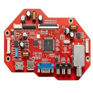
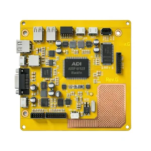
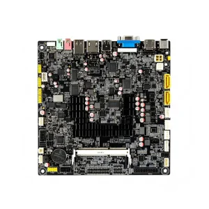
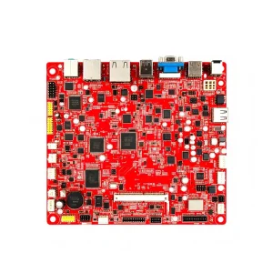
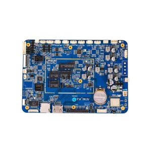
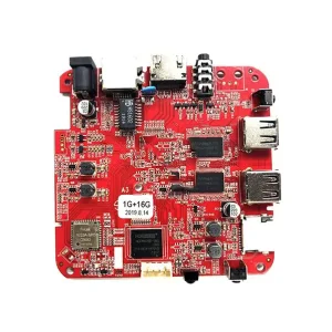
Explore our demonstrated execution across building automation, precision environmental monitoring, high-efficiency lighting, and vehicular control hardware.

Connect directly with our senior process engineers. Receive comprehensive DFM/DFA feedback, complete impedance modeling, and transparent turnkey quotations within 24 hours.
