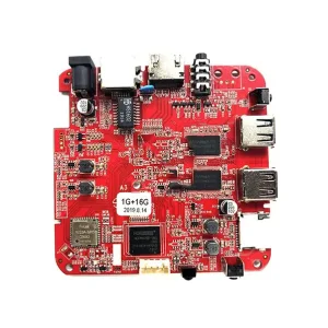
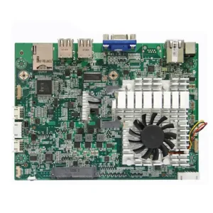
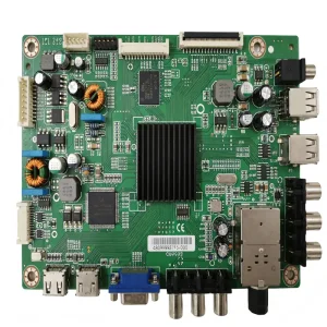
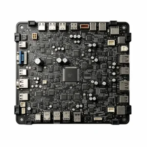
Explore our certified hardware designs, embedded processing architectures, and mission-critical assemblies deployed across global industrial, healthcare, and automotive systems.
From initial schematic capture to multilayer substrate manufacturing and zero-defect SMT assembly, Shenzhen STHL Electronics provides an uninterrupted engineering pipeline for mission-critical hardware.
In modern high-speed electronics, the boundary between circuit board design and manufacturing fabrication has vanished. Contemporary multi-gigahertz architectures, micro-pitch ball grid arrays (BGAs), and ultra-compact Internet of Things (IoT) nodes require every stage of the printed circuit board assembly (PCBA) to be tightly governed by Design for Manufacturability (DFM), Design for Assembly (DFA), and Design for Testability (DFT). When an engineering team drafts traces, creates differential pairs, or defines ground reference planes, real-world manufacturing constraints—such as dielectric dissipation factors ($Df$), copper roughness, etching undercut allowances, and reflow peak thermal deltas—directly dictate whether the prototype will function reliably in field operations.
Operating from our 10,000+ m² dust-free smart manufacturing facility in Bao'an, Shenzhen, Shenzhen STHL Electronics Co., Ltd. (founded in 2006) bridges high-level circuit concept formulation with turnkey volume manufacturing. Housing 7 high-speed SMT lines, 2 DIP/THT lines, 2 functional test lines, and 2 complete finished-device box-build assembly lines, STHL is powered by over 220 full-time specialists and an engineering department of 50+ seasoned hardware, layout, and manufacturing experts. By maintaining complete vertical control over component sourcing, bare-board multilayer fabrication, precision SMD placement, and end-of-line testing, STHL mitigates the structural risks typically caused by multi-vendor hand-offs.
Our engineering matrix spans advanced rigid, flexible, high-frequency RF, and heavy-copper thermal topologies engineered to satisfy rigid IPC Class 2 and Class 3 reliability criteria.
1+N+1 to Any-Layer microvia laser drilling, blind/buried vias down to 0.075mm, fine-line width/spacing down to 2.5/2.5 mil, accommodating 0.35mm pitch ultra-dense BGA footprints with automated optical inspection.
Controlled dielectric impedance ($Z_0 = 50\Omega \pm 5\%$, differential $100\Omega$) using low-loss Rogers 4350B, RO3003, Taconic, and Nelco high-speed PTFE substrates for 5G, radar, and aerospace avionic systems.
Up to 6oz outer/inner copper weights, aluminum core baseboards with 1.0–3.0 W/m·K thermal conductivity, direct thermal copper via stitching, and active heat-sinking for GaN/SiC power converters and EV charging stations.
Multi-layered polyimide flex cores bonded with FR-4 stiffeners for dynamic mechanical stress resilience, compact medical endoscopes, aerospace cockpits, and automotive vibration-prone assemblies.
Comprehensive pre-production engineering scrub checking for copper slivers, acid traps, solder mask bridges, annular rings, aspect ratio margins, component clearance, and bed-of-nails testpoint accessibility.
Electroless Nickel Immersion Gold (ENIG), ENEPIG for gold-wire bonding, Immersion Silver, Immersion Tin, and Lead-Free HASL optimized for fine-pitch SMT wetting, shelf life, and planar coplanarity.
Why Tier-1 global OEMs locate their core PCBA supply lines in Bao'an, Shenzhen—the undisputed epicenter of worldwide electronic manufacturing and components velocity.
Shenzhen’s industrial perimeter concentrates over 80% of the world's passive and active semiconductor logistical nodes. STHL maintains direct institutional relationships with authorized global franchises (including Arrow Electronics, Avnet, Digi-Key, Mouser, Farnell, Future Electronics, and Microchip Technology) alongside direct factory tier-1 silicon allocations.
With an active inventory catalog exceeding 500,000 components across 100+ vetted supply hubs, our automated procurement engine scans pricing indices, detects lead-time fluctuations, and flags End-of-Life (EOL) or Not Recommended for New Design (NRND) parts before purchase orders are issued. In times of global component crises, our procurement engineers secure authentic, traceable alternative parts with zero redesign penalty.
Fabricating high-layer-count substrates requires copper-clad laminates (CCL), photoresist films, and micro-drill consumables that reside within a 50-kilometer radius of our factory floor. While Western facilities face weeks of logistics latency simply securing Rogers high-frequency laminates or polyimide flex materials, our Shenzhen supply perimeter enables raw substrate arrival in under 24 hours.
This geographic density accelerates the New Product Introduction (NPI) cycle by up to 65%. Hardware startups and Fortune 500 enterprises can submit a Gerber package on Monday, receive deep DFM engineering feedback within 12 hours, complete laser bare-board fabrication by Wednesday, assemble 01005 passives and 0.35mm BGAs on Thursday, and receive fully inspected, flying-probe-tested functional prototypes across Europe or North America via DHL/FedEx by Friday morning.
Independent third-party audits ensure our production protocols align precisely with medical, automotive, and mission-critical industrial regulatory landscapes worldwide.
| Certification System | Target Industrial Sector | Manufacturing Controls & Quality Mandate | Audit & Traceability Protocols |
|---|---|---|---|
| IATF 16949 | Automotive & E-Mobility Subsystems | Automotive defect prevention, APQP, PPAP level 3 documentation, FMEA analysis, and sub-tier supplier control. | MES lot tracking, optical solder fillet verification, automated stencil wiping records. |
| ISO 13485 | Medical Devices & Life Sciences | Cleanroom assembly conditions, bio-burden mitigation, strict environmental tracking, and risk management (ISO 14971). | Device Master Record (DMR), Device History Record (DHR), and full lot-level component pedigree. |
| ISO 9001 | General Industrial & Enterprise OEM | Continuous improvement cycle, Kaizen waste elimination, operator calibration schedules, and vendor quality scorecards. | Internal bi-annual compliance audits and transparent corrective action request (CAR) cycles. |
| ISO 14001 | Environmental & Sustainability | Closed-loop effluent treatment, zero heavy-metal contamination, and lead-free RoHS/REACH substance management. | Hazardous materials certification, energy consumption reporting, safe e-waste disposition. |
| IPC-A-610 Class 2 & 3 | Avionics, Defense & High-Reliability | Zero-defect soldering criteria, through-hole barrel fill exceeding 75%, precise BGA voiding thresholds under 15%. | Certified IPC trainers on-site, 3D Automated Optical Inspection (AOI), and inline 3D X-Ray (AXI). |
To support global deployments without border friction, every PCBA delivered is accompanied by documentation proving conformity to CE (EMC Directive 2014/30/EU), FCC Part 15 Class A & B, UL 94V-0 flammability ratings, RoHS 3 (EU 2015/863), and REACH (EC 1907/2006). STHL works directly with accredited test laboratories including SGS, TÜV Rheinland, and Intertek, providing test-coupon cross-section analysis, ionic contamination testing, and solderability evaluations on every volume lot.
How our engineering and logistical architecture immunizes international purchasing directors against hidden supply line hazards.
The Risk: Offshore IP leakage, unauthorized firmware copying, and unauthorized third-party board manufacturing.
The STHL Safeguard: Before any Gerber files or schematics enter our secure portal, we execute a legally binding Non-Disclosure Agreement (NDA). Firmware flashing occurs inside closed, air-gapped MES-controlled programming cells with cryptographic token authentication. Hex files are automatically wiped post-flashing, and no design data leaves our internal firewall.
The Risk: Hidden solder voiding under large thermal pads and BGA spheres that lead to field failures under thermal cycling.
The STHL Safeguard: We utilize 10-zone nitrogen reflow ovens with real-time temperature profiling via KIC thermal loggers. Stencil apertures are micro-cut using nanocoated laser technology to optimize solder paste release. 100% of BGA and QFN packages pass through high-resolution 3D AXI (Automated X-Ray Inspection) with voiding strictly throttled below 15%.
The Risk: Sudden microchip discontinuation stalling an entire multi-million dollar product lifecycle.
The STHL Safeguard: Our engineering systems run predictive BOM health checks. If an MCU or driver IC is flagged for lifecycle transition, our team proposes pin-compatible, drop-in alternate parts, recalculates passive peripheral values, updates firmware drivers, and validates prototype equivalents before component stock dry-up occurs.
The Risk: Boards handcrafted in domestic prototype shops fail catastrophically when introduced to high-speed surface-mount lines.
The STHL Safeguard: With zero Minimum Order Quantity (MOQ), STHL runs your 5-piece functional prototype order on the exact same high-precision Yamaha and Fuji SMT lines used for 500,000-unit runs. Placement recipes, stencil apertures, and reflow recipes transfer seamlessly with 100% reproducibility.
The electronic hardware industry is undergoing massive structural transformations driven by artificial intelligence, wide-bandgap materials, and extreme miniaturization.
Deep-learning algorithmic routing engines predict parasitic capacitance, optimize return paths across split planes, and minimize crosstalk on high-speed DDR5/PCIe Gen 5 differential buses in seconds, dramatically reducing human design cycle hours.
Gallium Nitride and Silicon Carbide power stages switch at megahertz frequencies with unprecedented power densities. Modern circuit board design incorporates coin-embedded copper, thick-copper inner layers, and direct-bonded copper (DBC) ceramic substrates.
Blurring the line between IC packaging and bare boards, SLP enables sub-25µm lines and spaces using modified semi-additive processes (mSAP), allowing resistors and capacitors to be directly buried within inner prepreg layers.
Comprehensive, authoritative answers to critical inquiries raised by global hardware architects, compliance officers, and procurement managers.
To execute an end-to-end engineering assessment, we require: (1) RS-274X or ODB++ Gerber files specifying layer stack-ups, drill tables, and solder mask boundaries; (2) An engineering Bill of Materials (BOM) detailing exact Manufacturer Part Numbers (MPN), approved alternate manufacturers, reference designators, and package footprints; (3) A centroid (pick-and-place / XY data) file with rotational coordinates; and (4) An assembly and functional test specification detailing voltage thresholds, boundary scan requirements, and test fixture guidelines.
STHL maintains a zero-tolerance anti-counterfeit program in compliance with AS6081/AS5553 principles. All silicon and active devices are procured strictly through manufacturer-authorized distribution channels. In our internal incoming inspection lab, components undergo: microscopic marking verification, decapsulation acid analysis when applicable, solderability testing, lead coplanarity checks, and X-ray fluorescence (XRF) material composition verification to confirm RoHS conformity.
Yes. Our production floor runs state-of-the-art dual-lane modular pick-and-place machines capable of 01005 (0402 metric) ultra-miniature passive placement, 0.3mm pitch micro-BGAs, Package-on-Package (PoP) architectures, and odd-form connector insertions. For through-hole DIP components, we employ dual-wave selective soldering systems with programmable nitrogen shielding, ensuring optimal solder fillet elevation without subjecting surrounding delicate SMD parts to secondary thermal shock.
Our CAD/CAM layout engineers execute pre-layout and post-layout signal integrity (SI) and power integrity (PI) simulations using advanced industry modeling software. During bare-board multilayer lamination, test coupons are placed on the production panel border. We verify controlled single-ended ($50\Omega$) and differential ($90\Omega/100\Omega$) impedance traces using high-bandwidth Time Domain Reflectometry (TDR), delivering certified impedance test graphs with each shipment.
STHL offers an exhaustive testing regime: Automated Optical Inspection (3D AOI), inline 3D X-Ray Inspection (AXI), In-Circuit Testing (ICT), Flying Probe Testing for low-volume builds, In-System Programming (ISP), Functional Testing (FCT) using custom bed-of-nails or automated test racks, environmental thermal burn-in cycling (-40°C to +125°C), vibration profile testing, and high-voltage dielectric withstand (Hi-Pot) safety verification.
STHL enforces absolutely no Minimum Order Quantity (No MOQ). We assemble rapid-prototype quantities (from 1 to 5 boards) to empower hardware innovators to validate proof-of-concept designs. Once validated, those identical machine profiles, optical recipes, and component channels scale smoothly to mid-volume (5,000 units) and high-volume (100,000+ units) annual master purchase agreements on the same manufacturing floor.
For assemblies subjected to industrial chemicals, automotive under-hood exposure, or marine humidity, STHL operates automated selective conformal coating lines utilizing acrylics, silicones, polyurethanes, and UV-curable polymers (IPC-CC-830 certified). We also provide full silicone potting and encapsulation solutions to safeguard high-voltage circuits against moisture ingress, physical vibration, and dielectric breakdown.
Review additional examples of high-reliability telecom switches, automotive life-safety controllers, power modules, and specialized sensor assemblies manufactured in our facility.
Engage directly with our senior hardware and DFM engineering team in Shenzhen. Upload your Gerber, BOM, and assembly files for a confidential, NDA-backed technical assessment within 12 hours.