
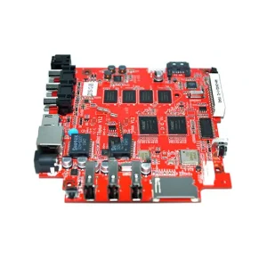
Explore qualified turn-key OEM PCB assemblies manufactured in our certified Shenzhen intelligent facility, adhering to rigorous zero-defect quality thresholds.
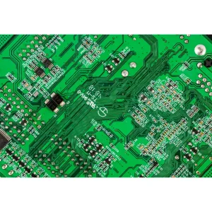
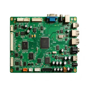
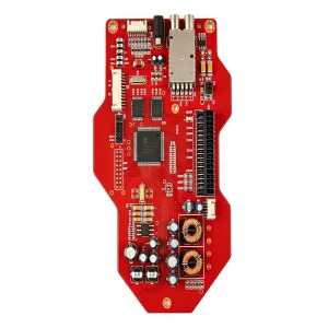
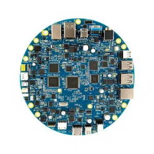
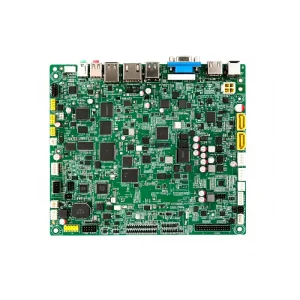
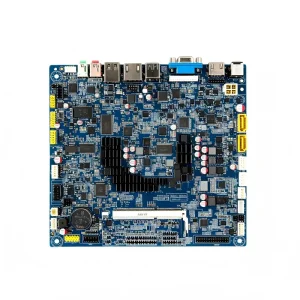
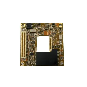
In modern electronics design and high-velocity product introductions, Original Equipment Manufacturers (OEMs) face compressing release cycles, escalating component obsolescence, and hyper-complex assembly specifications. Sourcing OEM Contract PCB Assembly is no longer simply an exercise in manual labor arbitrage; it has evolved into a strategic partnership driven by advanced automation, deep design-for-manufacturability (DFM) verification, and resilient supply chain integration.
Modern Chinese EMS facilities—centered primarily within the Greater Bay Area hardware cluster of Shenzhen and Dongguan—represent the most dense and agile electronics manufacturing ecosystem on the globe. Operating under international certifications such as IATF 16949, ISO 13485, ISO 9001, and ISO 14001, top-tier factories maintain high-speed Surface Mount Technology (SMT) lines capable of mounting 01005 passives and ultra-fine-pitch Ball Grid Arrays (BGAs) at defect frequencies well beneath acceptable IPC-A-610 Class 3 parameters.
Core Technical Value: "Turnkey Contract PCB Assembly in Shenzhen converges silicon procurement, multi-layer high-density interconnect (HDI) fabrication, automated optical/X-ray inspection, and system-level box build within a hyper-localized 50-kilometer radius, collapsing NPI engineering schedules from months to business days."
Instantaneous proximity to raw laminate producers, specialty chemistry formulators, passives authorized agents, and specialized tooling fabricators gives Chinese contract assemblers unmatched lead-time elasticity. Prototypes achieve quick-turn turnaround in 24 to 48 hours without compromising signal integrity validation.
Combating counterfeit semiconductors requires rigorous supply chain hygiene. Chinese EMS leaders connect through direct API lines to global distributors and verified local original component manufacturers (OCMs), backed by lot-level MES traceability, decapsulation spot-checks, and incoming X-ray fluorescence verification.
Transitioning seamlessly from New Product Introduction (NPI) pilot runs to high-volume production of hundreds of thousands of boards occurs under unified SPC (Statistical Process Control), closed-loop solder paste printing, nitrogen-inerted multi-zone reflow, and fully automated selective soldering setups.
Emerging architectures in electronic manufacturing services, driven by AI hardware acceleration, miniaturized high-voltage topologies, and uncompromising reliability mandates.
Traditional rule-based Automated Optical Inspection (AOI) suffers from false call rates exceeding 15% on high-density circuits. Advanced OEM contract factories now integrate 3D AI-powered vision algorithms trained on millions of solder bridge, tombstoning, and voiding parameters. Combining inline 3D AOI with automated 3D X-ray inspection (AXI) guarantees 100% volumetric joint inspection beneath bottom-terminated components (BTC), QFNs, and wafer-level CSP packages.
With the rapid proliferation of wide-bandgap semiconductors—specifically Gallium Nitride (GaN) and Silicon Carbide (SiC) switches—assemblies endure significantly higher power densities and thermal gradients. SMT lines now routinely assemble heavy-copper boards (up to 6oz), direct-bonded copper (DBC) ceramic boards, and insulated metal substrates (IMS), utilizing vacuum reflow soldering to limit thermal interface voiding below 5%.
The integration of wearable biomedical telemetry and edge-computing AI devices demands Package-on-Package (PoP) assemblies, 0.3mm pitch micro-BGAs, and 01005/008004 ultra-miniature passive chips. OEM factories deploy ultra-high-precision placement equipment featuring linear motor drives, nanometer optical feedback loops, and precision solder paste jetting to mitigate solder bridging on complex mixed-technology assemblies.
Global market access requires strict compliance with RoHS 3, REACH, and low-halogen directives. Contract PCB assembly factories must monitor peak reflow profiles precisely between 235°C and 250°C for lead-free alloys (SAC305, SAC0307) without subjecting temperature-sensitive components to thermal degradation, supported by real-time KIC thermal profilers and inert nitrogen soldering atmospheres.
| Manufacturing Dimension | Standard OEM Capability | Advanced / Class 3 Capability (STHL Standard) | Quality Verification Protocol |
|---|---|---|---|
| Min. Component Size | 0402 Imperial (1.0 × 0.5 mm) | 01005 Imperial (0.4 × 0.2 mm) & CSPs | High-Magnification 3D Optical Metrology |
| Fine Pitch IC Mounting | 0.5 mm Pitch BGA / QFP | 0.3 mm Ultra-Fine Pitch BGA & PoP | Volumetric 3D AXI (X-Ray) Void Analysis (<8%) |
| PCB Layer Stack-up | 2 to 16 Layers (Rigid FR-4) | Up to 64 Layers; HDI Any-Layer, Rigid-Flex | Cross-Section Microsectioning & TDR Impedance |
| Solder Atmosphere | Standard Convection Air | 10-Zone Nitrogen (N2) Reflow & Vacuum Solder | Oxygen PPM Monitoring (<500 ppm Residual) |
| Testing Coverage | Basic Functional Go/No-Go | Full Turnkey: Flying Probe, ICT, Boundary Scan, FCT | Custom automated test fixtures with cloud data logging |
Professional engineering and procurement executives evaluate contract assemblers through strict empirical parameters designed to eliminate supply chain fragility.
Tier-1 OEMs do not tolerate passive build-to-print suppliers. They require pre-production engineering teams that scrutinize Gerber files, drill layers, centroid data, and BOM components for solder starvation risks, component pad misalignments, shadow effects during wave soldering, and thermal imbalance across high-layer ground planes before a single panel is etched.
Single-source semiconductors introduce systemic delivery bottlenecks. A sophisticated China contract PCB assembly factory maintains in-house component engineering teams equipped to pinpoint Active End-of-Life (EOL) or Long-Lead components, suggesting drop-in Pin-to-Pin (P2P) functional equivalents and second-source alternatives without compromising system firmware compatibility.
Hardware innovation requires airtight legal safeguards. Global buyers require multi-tiered Non-Disclosure Agreements (NDAs) enforced prior to Gerber distribution, isolated factory sub-networks for proprietary firmware flashing, secure encrypted server silos for schematic storage, and segmented production cells for sensitive medical and defense-grade subassemblies.
Automotive and healthcare applications mandate forensic-level traceability. Advanced factories etch unique 2D DataMatrix barcodes on each individual PCB, logging feeder placement positions, reel lot numbers, reflow thermal curves, operator IDs, and test logs directly to an Enterprise Manufacturing Execution System (MES) retained for over 5 to 10 years.
How specialized contract manufacturing capabilities translate into field-ready mission-critical hardware across core international industrial sectors.
High-voltage Energy Storage Systems (BESS) and commercial photovoltaic inverters require assemblies engineered for severe dielectric isolation, creepage, and clearance safety. Contract assembly integrates heavy-copper busbar soldering, conformal polyurethane or silicone coating for anti-corrosion protection in salty outdoor atmospheres, and automated high-potential (Hi-Pot) surge isolation testing.
Regulated under ISO 13485 standards, medical PCBA demand zero-tolerance soldering stability. Applications ranging from bedside multiparameter patient monitors to ultrasound transducers require Class 3 precision SMT, automated ionic contamination testing to ensure zero ionic residue under IC bodies, and validated cleanroom assembly environments.
Industrial PLCs, motor servo drives, and environmental gas scrubbers operate continuously in environments subject to severe mechanical shock, particulate exposure, and broad thermal swings (-40°C to +105°C). Turnkey production incorporates robotic selective conformal coating, potting encapsulation, vibration testing, and extended high-temperature dynamic burn-in cycles.
Modern 5G enterprise routers, microwave links, and wireless signal boosters necessitate specialized hybrid laminates (e.g., Rogers combined with standard FR-4). Assembly involves controlled-impedance solder mask applications, precision blind and buried via backdrilling, micro-strip RF tuning, and dedicated RF Faraday cage transmission testing.
In-depth technical answers addressing engineering qualifications, component logistics, DFM feedback loops, and production economics.
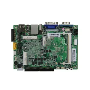
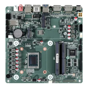
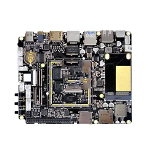
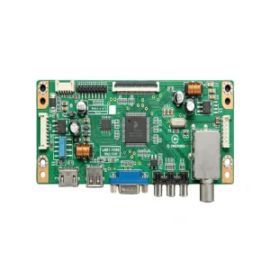
Specialized electronic manufacturing assemblies engineered for extreme industrial duty, medical diagnostics, and telecommunication infrastructure.

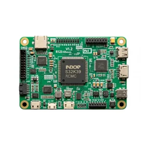
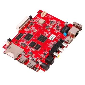
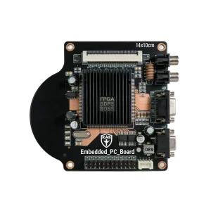
Submit your Gerber files, Bill of Materials (BOM), and mechanical tolerances for an authoritative Design-for-Manufacturability (DFM) review and comprehensive cost-optimized quote within 24 hours.