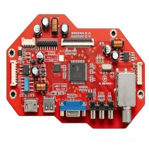
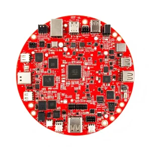
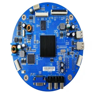
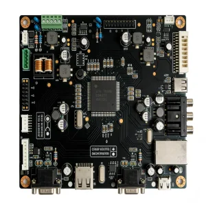
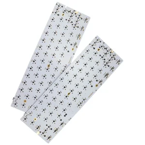
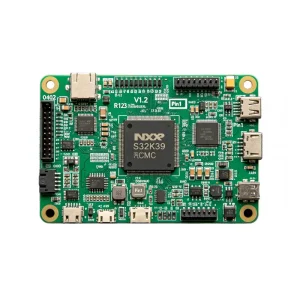
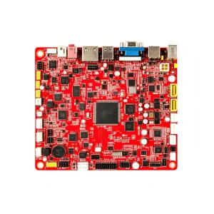
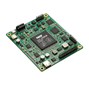
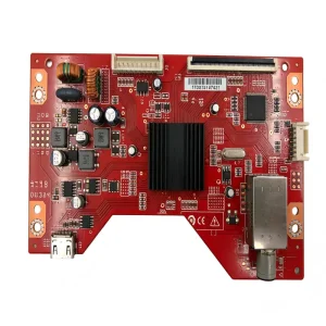
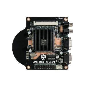
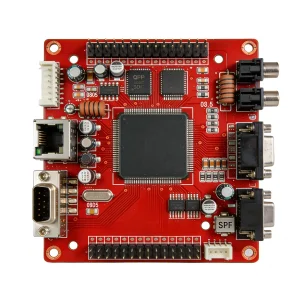
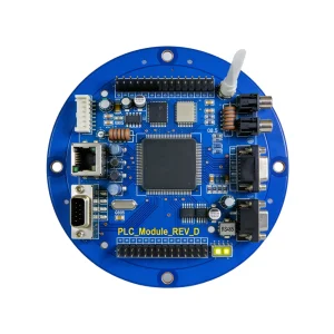
Explore our high-reliability, custom-engineered circuit modules running active DIP/THT configurations across mission-critical sectors.
While modern SMT micro-packaging addresses space-constrained consumer electronics, Dual In-Line Package (DIP) and Through-Hole Technology (THT) remain irreplaceable for high-voltage, extreme-vibration, and current-dense hardware architectures.
Unlike SMT solder joints that rely purely on copper foil surface adhesion, through-hole leads traverse the Plated Through-Hole (PTH) barrel. When soldered via selective or dual-wave soldering, the barrel forms an alloy intermetallic compound (IMC) that withstands severe mechanical shock up to 50G without micro-fracturing.
Heavy copper layers (up to 4oz–8oz) combined with thick-lead DIP components (power inductors, electrolytic capacitors, high-power MOSFETs) maximize thermal conduction through multi-layered inner thermal vias, transferring heat directly to heatsinks or aluminum backing.
Electronics exposed to field conditions—such as mining, maritime, aviation, and renewable energy substations—suffer from thermal fatigue and atmospheric corrosion. THT architecture enables deep conformal coating penetration and pot encapsulation.
Procuring custom DIP and mixed-assembly PCBA requires mitigating hidden engineering costs, single-source vulnerabilities, and lead-time volatility. Here is how modern EMS providers fulfill international procurement imperatives.
Procurement teams often suffer from localized price indexing. Our Design-for-Manufacturability (DFM) and Design-for-Assembly (DFA) analyses identify costly manual insertions and convert them into automated radial/axial insertions or selective-solderable footprints, trimming production costs by up to 28%.
With an active component network of 100+ authorized global distributors (including Arrow, Avnet, DigiKey, and Mouser), we guarantee 100% original traceable parts. Incoming material undergo X-ray fluorescence (XRF) testing, acetone decap testing, and microscopic lead inspection to prevent counterfeit penetration.
OEMs demand seamless product lifecycles. We support fast rapid prototyping (NPI) within 3-5 days and transition straight into automated wave-soldering mass lines without re-qualifying tooling fixtures, removing transition risk and preserving time-to-market.
| DIP / THT Capability Parameter | Standard OEM Industry Metric | Advanced Industry 4.0 Factory Standard |
|---|---|---|
| Soldering Methodology | Manual Soldering / Standard Wave Solder | Automated Nitrogen (N2) Selective Wave Soldering |
| PTH Hole Barrel Fill Ratio | ≥ 50% (IPC Class 2 Baseline) | ≥ 75% to 100% (IPC-A-610 Class 3 High Reliability) |
| Component Pitch Support | Pitch ≥ 2.54mm | Ultra-Fine Pitch Down to 1.27mm / Staggered Formations |
| Lead Forming & Trimming | Manual Hand Tools & Gauges | Automated CNC Optical Forming & Auto-Cut Systems |
| Post-Assembly Inspection | Manual Visual Inspection (MVI) | High-Speed 3D AOI + Automated 3D X-Ray (AXI) |
| Component Traceability | Batch Lot Code Recording | Unit-Level 2D DataMatrix Tracking via Cloud MES |
Shenzhen represents the epicenter of the global electronics industrial complex. Operating from our 10,000+ m² smart factory, we harness the unmatched density of the Greater Bay Area hardware cluster to deliver velocity and cost control.
Within a 30-kilometer radius in Bao'an, Shenzhen, our facility connects directly to precision plastic molders, metal CNC stamping shops, bare PCB fabricators, custom transformer winders, and connector foundries. This structural advantage reduces engineering lead times from months to days.
Our dual-wave and selective wave soldering lines integrate intelligent nitrogen atmosphere chambers that run under 50 PPM residual oxygen. This setup completely eliminates solder dross and micro-bridging. Real-time sensor arrays stream soldering thermal curves directly into our MES system.
Every DIP board is laser-engraved with an individual barcode at the bare PCB stage. As components pass through auto-insertion, hand-stuffing stations, selective soldering, 3D AOI, and functional test (FCT) jigs, each process metric is locked to that serial number for lifetime traceability.
Across power distribution, medical systems, industrial automation, and renewable energy, our custom DIP assembly is tailored to exact domain challenges and certification frameworks.
Wind turbine controllers, solar micro-inverters, and EV charging stations require massive power throughput. We execute thick-copper (4–6 oz) through-hole soldering with specialized solder wave pallet jigs that ensure full thermal saturation without scorching adjacent SMT micro-chips.
Patient monitors, surgical power devices, and dialysis machinery demand zero tolerance for signal drift and electrical leakage. Our ISO 13485 certified lines maintain strict electrostatic discharge (ESD) regimens and low-ionic contamination thresholds.
Factory automation systems face continuous mechanical vibration, electrical noise, and airborne oil vapor. We reinforce high-mass relays, large input inductors, and terminal blocks using secondary silicone anchors and mechanical pin cinching.
Cross-border electronics manufacturing demands uncompromising compliance frameworks and transparent communication. We bridge engineering gaps through dedicated bilingual PM teams and globally recognized certifications.
Our manufacturing workflow is certified under IATF 16949 (Automotive Quality Management), ISO 13485 (Medical Devices), ISO 9001 (Global QMS), and ISO 14001 (Environmental Safety). We conduct annual third-party audits to guarantee adherence to rigorous standards.
We treat intellectual property as your core asset. Strict NDAs precede any Gerber or firmware data exchange. Factory network topologies physically isolate client firmware burning stations, ensuring cryptographic keys and compiled binaries remain secure.
Our global shipping matrix provides end-to-end Delivered Duty Paid (DDP) logistics directly to warehouse docks in over 90 countries. We guarantee full conformity with RoHS 3, REACH, CE, UL94V-0 flame retardancy, and WEEE electronic waste regulations.
As power electronics migrate to Wide-Bandgap (WBG) semiconductors like Gallium Nitride (GaN) and Silicon Carbide (SiC), DIP technology is adapting to elevated frequencies, intense thermal density, and autonomous assembly protocols.
Next-generation high-frequency power switching devices demand low parasitic inductance. Our engineering team is developing localized shielding around through-hole pins and implementing customized copper press-fit pins that bypass solder reflow cycles entirely, minimizing parasitic inductance while boosting efficiency.
Transitioning beyond traditional 2D optical thresholding, our factory deploys deep-learning neural networks trained on over 2 million solder joint images. This AI engine evaluates meniscus concave curves, wettability angles, and sub-surface porosity on X-ray cross sections with a false call rate below 0.05%.
In response to global sustainability initiatives and delicate thermal budgets on hybrid SMT/DIP assemblies, our metallurgical laboratory is qualifying Bismuth-Tin-Silver (Sn-Bi-Ag) micro-alloy wave solder formulations that melt below 180°C, lowering energy consumption while preventing component warpage.
Review the second series of our high-durability assemblies, running in monitoring, green energy, telecommunications, and high-frequency power supplies worldwide.
Clear, direct answers for engineering directors, sourcing leads, and procurement managers evaluating factory capabilities.
Upload your Gerber files and BOM. Our senior DFM engineers will conduct a full stack-up feasibility, thermal profile assessment, and component lead-time analysis within 24 hours.