Engineered to deliver high thermal stability, minimal signal loss, and zero-defect operational durability across complex operational environments.
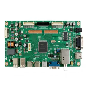
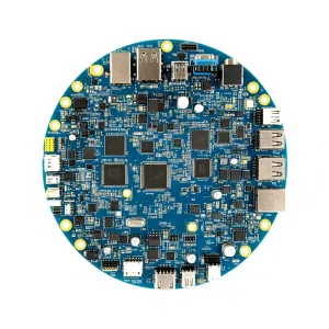
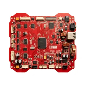
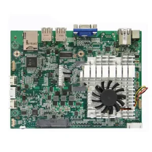
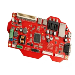


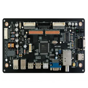
In modern electronic circuit manufacturing, transitioning from functional prototypes to mass production requires strict thermal profiling, micro-pitch component placement, and integrated quality feedback mechanisms.
Utilizing high-speed, multi-module mounters equipped with dual-vision alignment systems, production achieves stable placement down to 01005 passive chips and 0.3mm pitch fine-pitch Ball Grid Arrays (BGA). Closed-loop linear encoders guarantee repeatable placement tolerances within ±0.025mm across diverse panel sizes.
Prior to tooling, every Gerber layer, IPC-7351 footprint, and Bill of Materials (BOM) undergoes automated Design for Manufacturability (DFM) analysis. Potential solder bridging, tombstoning hazards, thermal imbalance, and mechanical clearance violations are eliminated before stencils are cut or copper clad is milled.
Multi-zone nitrogen-purged (N2) reflow ovens with real-time profiling suppress oxidation during liquidus peak temperatures. This process maintains optimal wetting angles for lead-free SAC305 and low-temperature alloys, minimizing intermetallic compound (IMC) brittleness and eliminating micro-voiding beneath large QFN thermal pads.
Strategic geographic location in the Greater Bay Area delivers unparalleled component liquidity, reducing prototype turnaround times from months to days while defending production schedules against localized shortages.
Our centralized procurement network interfaces directly with authorized master distributors (such as Arrow, Avnet, Mouser, Digi-Key, STMicroelectronics, and TDK) as well as audited domestic semiconductor packaging houses. Accessing over 500,000 verified line items ensures rapid alternate sourcing for End-of-Life (EOL) or active allocations, neutralizing long lead-time risks.
By synchronizing raw FR-4/Rogers substrate fabrication, laser-cut electro-polished stencils, precision injection-molded housings, custom cable harnesses, and final robotic enclosure assembly within a 20-kilometer radius, production cycles drop from traditional 8-week turnarounds to sub-15-day complete runs without compromising IPC Class 2 or Class 3 reliability metrics.
From initial design intake to palletized global shipping, every stage is enforced by Enterprise Resource Planning (ERP) and Manufacturing Execution Systems (MES) logging.
100% incoming component inspection, verification of moisture sensitivity levels (MSL), baking protocols, and XRF spectrometer testing to prevent counterfeit components.
Inline 3D SPI measures paste volume, height, area, and registration offset across every pad, catching up to 70% of potential surface mount soldering anomalies before reflow.
Post-reflow 3D Automated Optical Inspection verifies component presence, polarity, skewed bodies, solder bridging, insufficient fillets, and tombstoning at high throughput.
Non-destructive X-ray laminography inspects hidden solder joints on BGAs, CSPs, and leadless QFNs, verifying voiding ratios remain strictly within IPC-A-610 Class 3 specifications.
Custom bed-of-nails fixtures, Boundary Scan (JTAG), automated firmware flashing, and full parametric environmental stress screening (ESS) ensure field-ready assemblies.
Quantitative benchmarks across printed circuit board fabrication, surface mount assembly, and selective soldering processes.
| Process Parameter | Standard Capability | Advanced / High-Density Capability | Compliance Standards |
|---|---|---|---|
| Min Component Pitch | 0.4mm (BGA), 0.3mm (Lead) | 0.3mm (BGA), 0.25mm (CSP/Micro-BGA) | IPC-7351B |
| Smallest Passive Device | 0201 (Imperial) / 0603 (Metric) | 01005 (Imperial) / 0402 (Metric) | IPC-A-610 Class 3 |
| PCB Substrate Topologies | FR-4, High-Tg (TG170/180), Aluminum Core | Rogers High Frequency, Polyimide Flex, Rigid-Flex, HDI Any-Layer | UL 94V-0 |
| Surface Finishes | HASL, Lead-Free HASL, OSP | ENIG, ENEPIG, Immersion Silver, Immersion Tin, Hard Gold Plating | RoHS / REACH |
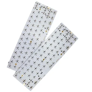
| Max Board Dimensions | 510mm × 460mm | 1200mm × 350mm (Ultra-long LED panels) | SMEMA Standard |
| Traceability & Tracking | Batch Lot QR / Barcode Tracking | Individual Laser 2D DataMatrix Tracking linked to full MES log | IATF 16949 / ISO 13485 |
Bridging overseas design teams with domestic manufacturing scale through dedicated Field Application Engineers (FAE) and rigorous industry certifications.
Every automotive assembly adheres to strict Advanced Product Quality Planning (APQP), Production Part Approval Process (PPAP Level 3), Failure Mode and Effects Analysis (FMEA), and total statistical process controls (CpK > 1.67) to fulfill mission-critical in-vehicle safety tolerances.
Designed for diagnostic instrumentation and patient-monitoring electronics, our manufacturing cleanrooms follow documented change controls, device history record (DHR) tracking, risk mitigation routines, and full bio-compatibility material verification.
Direct communication with certified FAE and project management engineers eliminates translation barriers. Engineering inquiries, thermal simulation data, and alternate BOM sign-offs are processed in real time across North American, European, and Asia-Pacific business hours.
The convergence of edge AI acceleration, wide-bandgap semiconductors, and extreme miniaturization is redefining electronics manufacturing processes.
Next-generation DC-DC converters and high-efficiency power supplies demand lower parasitic inductance. Assembly strategies incorporate direct thermal vias, thick copper (up to 6oz) planes, and vacuum-assisted vapor phase soldering to dissipate extreme heat densities without thermal degradation.
As IoT nodes and smart sensors contract in form factor, multi-stage laser-drilled microvias, staggered/stacked configurations, and copper-filled via-in-pad plating (VIPPO) allow active components to be positioned directly above routing layers, reducing overall assembly footprint by over 40%.
To eliminate manual soldering inconsistencies across high-mass connectors and sensitive through-hole headers, automated multi-axis selective soldering machines utilize individual nitrogen blankets and precision spray fluxing to guarantee repeatable 100% vertical barrel fill.
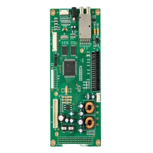
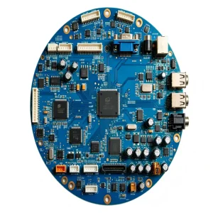
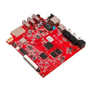
Discover our proven turnkey assemblies engineered for robotics, photonics, radiation monitoring, and critical automotive applications.
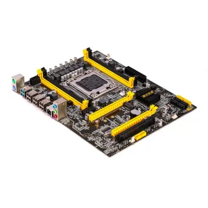

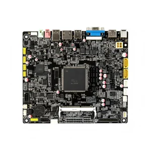
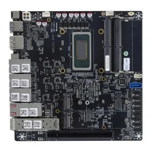
Clear, direct answers for engineering directors, procurement managers, and hardware designers evaluating custom circuit assembly partnerships.
Upon receiving your package (Gerber RS-274X or ODB++, bill of materials with active Manufacturer Part Numbers, centroid XY pick-and-place files, and assembly schematics), our FAE team conducts a thorough 48-point check. This includes verifying copper clearance, trace aspect ratios, annular rings, solder mask web width, stencil aperture-to-pad ratios, component aspect ratios, and shadowing effects during reflow to prevent rework during high-volume production.
We operate an audited procurement workflow conforming to AS6081 and IDEA-STD-1010 standards. All silicon, passives, and electromechanical components are procured through authorized franchised distribution or direct original component manufacturers (OCM). When obsolete components must be acquired from secondary channels, parts undergo external visual inspection, marking permanency testing, decapsulation, die verification, and X-ray lead-frame analysis before entering production stock.
We provide full-spectrum testing based on customer requirements: In-Circuit Testing (ICT) via dedicated bed-of-nails or flying probe fixtures, Boundary Scan (JTAG), automated In-System Programming (ISP), Functional Testing (FCT) simulating real-world operational loads, Dielectric Withstand Voltage (Hipot), and Environmental Stress Screening (thermal cycling, damp heat, and vibration testing according to IEC 60068).
We enforce a strict No Minimum Order Quantity (No MOQ) policy. High-mix low-volume (HMLV) engineering runs and pilot builds utilize the exact same precision surface mount equipment, reflow profiles, and automated optical validation systems as mass-volume automotive runs. This ensures a seamless transition to high-volume manufacturing without requalification or redesign delays.
Confidentiality is secured via binding Non-Disclosure Agreements (NDAs) executed prior to file transmission. Internal data governance isolates engineering designs, Gerber files, and proprietary BOMs on encrypted servers with role-based access. Firmware programming stations operate on sandboxed local networks, logging MAC addresses, flash verification checksums, and unit serializations without internet access, preventing unauthorized firmware extraction or overproduction.
