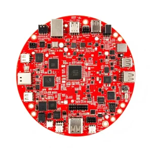
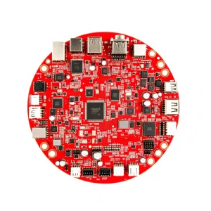
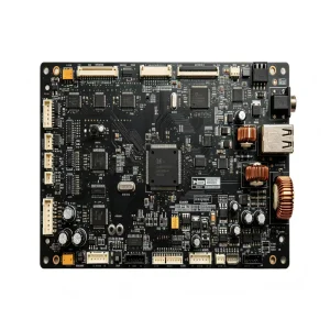
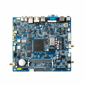
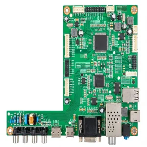
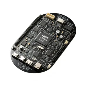
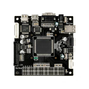
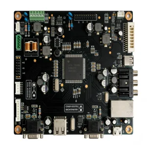
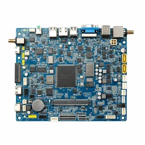
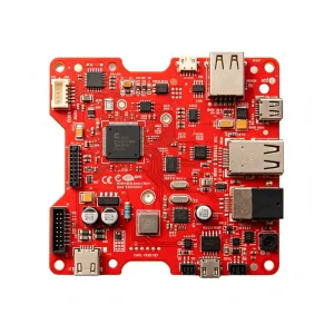
Precision-manufactured electronic assemblies built to IPC-A-610 Class 3 specifications for mission-critical industrial, medical, and control applications.
Navigating technical convergence: How high-density interconnects, edge computing, and component volatilities dictate contemporary manufacturing paradigms.
Modern electronics demand radical board miniaturization without signal degradation. Our manufacturing capabilities accommodate Any-Layer HDI, blind and buried micro-vias, and fine-pitch wafer-level packaging. Rigorous control of thermal profiles during multi-stage reflow processes ensures structural solder joint integrity for complex systems-on-chip (SoCs) and power ICs.
From high-efficiency power distribution networks to high-current Battery Management Systems (BMS), managing localized heat dissipation is imperative. We utilize heavy-copper substrates (up to 4oz+), ceramic-core PCBs, and integrated aluminum backing to facilitate high thermal conductivity, directly addressing the requirements of mission-critical converters and inverters.
Electronics manufacturing extends beyond bare PCBA surface mounting. Turnkey box build capabilities synthesize structural CNC machining, injection-molded plastics, cable harness engineering, automated conformal coating, and pot encapsulation. Single-point architectural assembly eliminates inter-vendor tolerance mismatches and guarantees operational ruggedness.
Shenzhen's manufacturing cluster remains unmatched in global throughput, vertical ecosystem integration, and rapid cycle times from New Product Introduction (NPI) to mass scaling.
Every PCBA moving across our SMT lines undergoes multi-angle inline 3D AOI to capture volumetric paste irregularities, misalignment, and tombstoning. For BGA, QFN, and bottom-terminated components, high-resolution 3D AXI verifies solder joint voiding rates below 10%, mitigating field failure modes caused by latent mechanical or thermal stress.
Operating within the Pearl River Delta provides direct, verified distribution pipelines for hard-to-source active components, MLCCs, connectors, and passives. Supported by a database of over 500,000 components and formal franchise authorizations, we mitigate counterfeit risks with incoming XRF spectroscopy, decapsulation, and acetone solder testing.
Traceability is the cornerstone of Tier-1 contract manufacturing. Our Manufacturing Execution System (MES) assigns custom barcode identifiers to each PCB panel, indexing individual component lot reels, operator IDs, reflow temperature profiles, and functional test data points. This guarantees complete lifecycle visibility for audit defenses.
Harmonizing international regulatory frameworks to ensure risk-free global market entry across North America, the European Union, and Asia-Pacific.
Meeting zero-defect mandates within the automotive electronics sector requires rigorous implementation of APQP, FMEA, MSA, and PPAP. Solder deposition, component placement forces, and selective soldering processes are strictly managed to withstand severe vibration, wide temperature cycling (-40°C to +125°C), and environmental extremes.
Medical hardware leaves no margin for error. We operate under stringent cleanroom handling, bio-burden controls, and comprehensive engineering change order (ECO) management. From diagnostic displays to surgical control suites, each assembly adheres to FDA QS-Reg/MDR specifications and risk mitigation guidelines.
We deploy closed-loop lead-free (Pb-Free) soldering lines adhering strictly to EU RoHS 3 and REACH compliance. Waste disposal, solvent vapor extraction, and water cleaning systems are certified according to ISO 14001, providing international partners with verifiably green and ethically managed supply chains.
Clear, engineering-focused answers to critical concerns regarding IP security, testing coverage, component lifecycles, and NPI ramp-up.
Intellectual Property security is strictly institutionalized. Prior to accessing your Gerber or BOM data, legally binding bilateral NDAs are enacted. Firmware programming is executed within network-isolated flashing stations, ensuring hex files are never exposed to unauthorized personnel or external networks.
Our engineering team delivers a comprehensive Design for Manufacturing (DFM) and Design for Testing (DFT) report within 24 to 48 hours of RFQ submission. We analyze trace clearance, aspect ratios, solder mask slivers, component footprint overlaps, thermal reliefs, and test point accessibility.
We actively monitor component lifecycle statuses (End-of-Life, Not Recommended for New Designs). Our component engineering group provides verified form-fit-function (FFF) alternative proposals, cross-referencing datasheets, pinouts, and electrical parameters to prevent production halts.
Beyond standard AOI, SPI, and 3D X-ray inspection, we design customized Functional Test (FCT) jigs, In-Circuit Testing (ICT), Boundary Scan, and Burn-in stress testing (thermal chamber temperature cycling). Firmware flashing, RF spectrum verification, and dielectric breakdown testing are fully accommodated.
Explore our demonstrated mass-production assemblies deployed in telecommunications, automotive electronics, environmental monitoring, and connected devices.