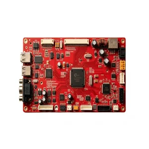
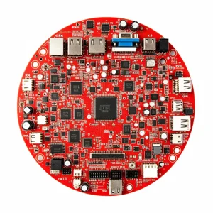
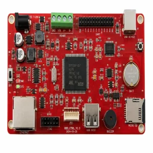
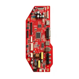
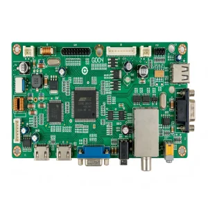
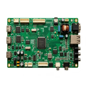
Explore our industrial-grade, certified PCBA manufacturing solutions engineered to exceed stringent mission-critical demands.
Analyzing the pivotal shifts reshaping global hardware manufacturing, from multi-die packaging to extreme thermal management.
The push for miniaturized consumer edge devices and automotive ECUs necessitates complex micro-via HDI technology, multi-layer rigid-flex integration, and flawless 01005 passives placement without thermal bridging or tombstoning defects.
High-voltage converters and solar inverters transition rapidly to Gallium Nitride (GaN) and Silicon Carbide (SiC) architectures. As thermal flux escalates, OEM assembly demands automated vacuum reflow and copper substrate heat distribution.
Compliance across critical medical (ISO 13485) and automotive (IATF 16949) sectors mandates end-to-end component lifecycle provenance, non-destructive 3D CT X-ray inspection, and comprehensive environmental protection using automated conformal coating.
Addressing the top challenges facing VP-level procurement and supply chain executives in a volatile global market.
Global procurement teams prioritize deep-tier traceability. Our API integration with authorized global distributors (Arrow, Avnet, DigiKey) combined with incoming destructive/non-destructive lab verification prevents fraudulent or gray-market silicon infiltration.
Beyond the piece-part price, forward-thinking procurement evaluates yield rates, assembly cycle time, and rework overhead. Proactive Design for Manufacturing (DFM) audits systematically reduce assembly steps and minimize yield loss before initial prototype spins.
Shorter device lifecycles demand instantaneous scaling without switching assembly partners. We eliminate friction by using identical automated SMT lines for rapid 24-hour prototype batches and full-scale monthly runs exceeding 500,000 units.
Combining the world's most concentrated component clusters with advanced AI-driven process automation.
Our 10,000+ m² facility features high-speed Yamaha and Fuji pick-and-place systems. Integrated 3D SPI (Solder Paste Inspection) and multi-angle 3D AOI identify bridging, skew, coplanarity deviation, and micro-voids prior to high-temperature reflow.
Situated in the heart of the Greater Bay Area, our sourcing hub commands direct, real-time access to passives, bare boards, semiconductors, custom plastics, and metal CNC tooling. Sourcing cycles drop from weeks to hours, ensuring agile mitigation against supply shocks.
Every PCBA moving across our SMT, DIP, Conformal Coating, and Box Build cells is marked with an irreversible 2D DataMatrix code. We track solder lot, reflow thermal profiles, operator IDs, and automated functional testing vectors with zero data leakage.
Engineered to perform in severe physical, thermal, and electromagnetic environments across industrial landscapes.
For aerospace and robotic INS modules, vibration damping, zero-flux contamination, and high-frequency RF trace shielding are critical. Our specialized underfill application protects high-pin BGA devices against continuous dynamic g-forces.
Renewable power electronics demand thick copper (3oz–6oz) boards, wide track clearances, and high creepage insulation. We integrate selective soldering, potting, and automated high-potential (Hi-Pot) safety testing up to 5,000V DC.
Non-invasive patient monitoring and vital diagnostic instrumentation demand precise low-noise routing, gold surface finishes (ENIG/ENEPIG), and bio-compatible conformal coatings compliant with strict ISO 13485 production procedures.
Comprehensive answers covering design transfer, engineering validation, quality gates, and IP safeguarding.
We provide complete turnkey electronic contract manufacturing: early DFM/DFT analysis, PCB fabrication, BOM sourcing, high-speed SMT/THT insertion, firmware flashing, conformal coating, cable harnessing, structural box build, and full functional testing (FCT).
Upon receiving your Gerber, BOM, and centroid files, our engineers review footprint clearances, thermal reliefs, solder paste apertures, and component availability. Identifying layout snags before tooling prevents costly revisions down the road.
We enforce a strict No-MOQ policy. We support hardware startups and enterprise R&D groups with 5-piece prototype validation runs, maintaining identical process controls and machines when scaling up to millions of mass-production units.
Our operations are certified under IATF 16949 (Automotive), ISO 13485 (Medical), ISO 9001, and ISO 14001. Quality screening includes 3D SPI, automated optical inspection (AOI), 2D/3D X-Ray inspection, in-circuit test (ICT), and customer-specified burn-in.
All sensitive design data is protected under robust Non-Disclosure Agreements (NDAs). Firmware programming occurs within segregated, encrypted networks, and server-side access to customer Gerber and BOM files is restricted to assigned project engineers.
We source exclusively through direct semiconductor manufacturers and franchise distributors. When components face end-of-life (EOL) or allocations, our component engineering team recommends pin-compatible drop-in replacements with verified specs.
To produce an engineering DFM and quotation within 24–48 hours, we require: 1) RS-274X or ODB++ Gerber files, 2) Comprehensive BOM with exact Manufacturer Part Numbers (MPN), 3) Centroid / Pick-and-Place data, and 4) Testing & Assembly requirements.
All finished assemblies are vacuum-sealed in ESD-safe, anti-moisture barrier packaging with desiccant and humidity indicator cards. We deliver reliably across 90+ countries via DHL, FedEx, air freight, or ocean consolidations, backed by a 99.5% on-time record.
From biometric sensors to aviation navigation and smart power conversion—discover additional tailored manufacturing solutions.