
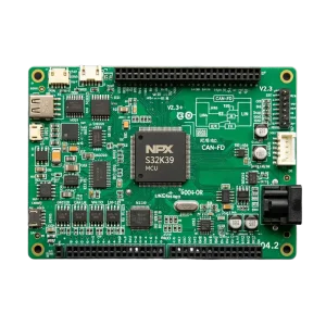
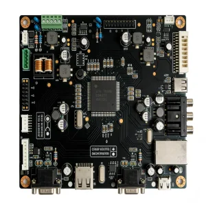
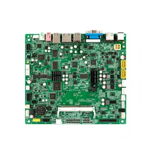
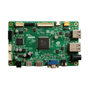
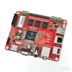
Real-world printed circuit board assembly prototypes manufactured under zero-defect containment protocols for commercial and mission-critical applications.
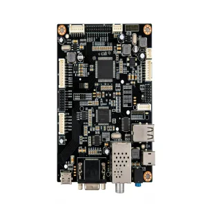
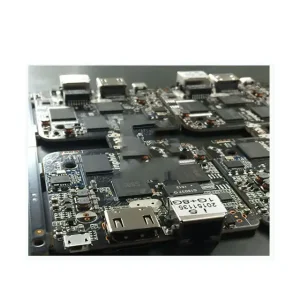
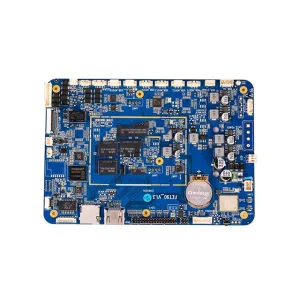

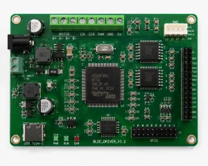
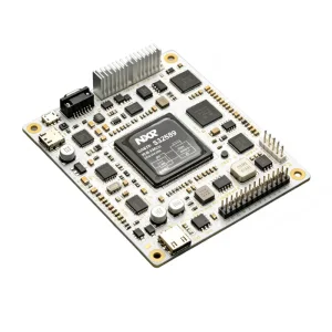
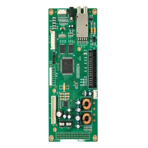
Why tier-1 electronics enterprises are transitioning from transactional, low-cost assembly vendors to specialized engineering fabrication partners.
Global hardware teams no longer operate within 6-month product update horizons. Rapid prototype iterations in 24 to 72 hours determine time-to-market dominance in AI compute, automotive ADAS, and IoT devices. The demand focuses on fast turn-around without compromising manufacturing design rules.
Fragmented sourcing frequently delays assembly. Procurement requirements prioritize manufacturers offering real-time component lifecycle analysis, algorithmic alternative sourcing (pin-to-pin drop-in replacements), and certified anti-counterfeiting verification straight from authorized distribution tiers.
A bare prototype that cannot scale efficiently causes massive fiscal drain during pilot runs. Modern procurement mandates deep-level Design for Manufacturability (DFM) and Design for Assembly (DFA) feedback within 12 hours of file submission, neutralizing copper clearance, thermal relief, and solder bridging risks upfront.
Bridging theoretical CAD layouts with physical manufacturing reality through scientific metallurgical control, high-density placement, and multi-tier verification.
STHL deploys advanced high-speed surface-mount platforms capable of placing 01005 passives and 0.3mm ultra-fine pitch Ball Grid Arrays (BGAs). Prototyping runs undergo automatic 3D SPI (Solder Paste Inspection), dynamic thermal reflow profiling, and multi-angle 3D Automated Optical Inspection (AOI) to eliminate non-wetting and bridging.
Handling blind, buried, and stacked micro-vias down to 0.075mm via laser direct imaging. Our fabrication facility processes standard FR-4, High-Tg (TG170/TG180), Rogers RF substrates, polyimide flexible printed circuits (FPC), and metal core (IMS) platforms, strictly maintaining targeted characteristic and differential impedance within ±7%.
High-density prototypes cannot rely solely on optical clearance. Every prototype batch with active arrays or concealed pad terminations passes real-time industrial transmission 2D/3D X-ray inspection to gauge solder ball voiding against IPC-A-610 Class 3 criteria (<15% threshold) ensuring maximum mechanical and thermal integrity.
Real capability metrics verified in production for mission-critical hardware design engineers.
| Process Parameter | Quick-Turn Prototype Standard | Advanced / High-Density Capability | Validation & Inspection Gate |
|---|---|---|---|
| Layer Count Range | 1 – 8 Layers (24h - 48h Turn) | Up to 64 Layers, Any-Layer HDI (1+N+1 to 4+N+4) | Cross-Section Micro-etch Analysis |
| Min Trace Width / Spacing | 3.0 mil / 3.0 mil (0.075mm) | 1.8 mil / 1.8 mil (0.045mm) on thin Cu foil | Laser Automated Optical Metrology |
| Surface Mount Pitch | 0.4mm pitch (QFP, BGA, WLCSP) | 0.3mm pitch micro-BGA & 01005 Passives | 3D Solder Paste & High-Res 3D AOI |
| Blind / Buried Via Aspect Ratio | 1:1 (Laser micro-vias) | 1:0.8 to 1:1.2 with VIPPO (Via-in-Pad Copper Plated) | Transmitted 3D X-Ray Inspection |
| Controlled Impedance | ±10% Standard Single/Differential | ±5% Precision Controlled (Polar Si9000 Verified) | Time-Domain Reflectometry (TDR) |
| Soldermask Registration | ±2 mil (0.050mm) | ±1 mil (0.025mm) via LDI Exposure | Microscope Optical Alignment |
| Functional Testing | Flying Probe Test & Boundary Scan | Custom Bed-of-Nails & Functional Firmware Execution | 100% In-Circuit & Electrical Continuity |
Bridging global engineering footprints with strict intellectual property isolation and internationally recognized manufacturing credentials.
Proprietary Gerber files, schematic diagrams, and customized firmware payloads represent critical enterprise capital. STHL operates on an encrypted, access-segmented internal server infrastructure. Engineering reviews begin exclusively following a formal, mutually executed Non-Disclosure Agreement (NDA).
STHL maintains continuous, audited compliance covering IATF 16949 (Automotive Electronics Quality Management), ISO 13485 (Medical Device Manufacturing), ISO 9001, and ISO 14001. Material sourcing ensures stringent RoHS and REACH environmental regulatory compliance without regional ambiguity.
Shipping precision prototypes across North America, the European Union, the United Kingdom, and Asia-Pacific through direct priority air networks. Every work order features end-to-end cloud ERP traceability, ensuring customs clearance manifests, batch certificates of conformance (CoC), and full material test reports.
Scaling seamlessly from verified rapid prototypes to high-volume recurring electronic manufacturing operations.
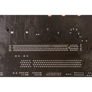
Direct, unambiguous technical answers regarding prototype validation, manufacturing rules, and production escalation.
Our rapid prototyping speed relies on dedicated NPI fast-track lines separate from standard mass-production runs. We maintain an in-house inventory of over 500,000 standard passive and active electronic parts, utilize quick-setup Panasonic and Yamaha SMT placement platforms, and run automated DFM verification pipelines immediately upon receiving CAD/Gerber packages. Bare boards are expedited through localized high-speed laser direct imaging (LDI) lines.
To provide a fully verified quotation and DFM analysis within 12 to 24 hours, our engineering staff requires: (1) RS-274X or ODB++ Gerber files with layer stack-up definitions, (2) A consolidated Bill of Materials (BOM) including Manufacturer Part Numbers (MPN) and authorized substitute rules, (3) Centroid / Pick-and-Place data (X-Y coordinates and rotation), and (4) Special assembly instructions such as conformal coating boundaries, press-fit tolerances, or functional testing programs.
Our procurement system monitors live API interfaces with major tier-1 semiconductor channels (including Arrow, Avnet, DigiKey, Mouser, and verified franchised manufacturers). When an active IC or MCU is designated End-of-Life (EOL) or carries unacceptable lead times, our component engineering division provides drop-in pin-compatible alternatives, minor layout adjustment recommendations, or conducts authenticated broker verifications backed by decapsulation and XRF testing.
Prototypes manufactured at STHL are built on the same certified SMT lines that run our volume production. Medical devices comply strictly with ISO 13485 clean handling, device history tracking, and component traceability protocols. Automotive prototypes fall under IATF 16949 quality guidelines, adhering to IPC-A-610 Class 2 or Class 3 workmanship criteria, complete with documented thermal solder reflow logs and 100% X-ray inspection of concealed joints.
Yes. Eliminating the friction between prototype labs and production factories is our fundamental value proposition. Because our NPI engineers record every production detail—stencil aperture design, reflow profiling temperatures, feeder arrangements, and test fixtures—within our unified MES (Manufacturing Execution System), scaling from 5 to 500,000 units requires zero retraining or transfer re-qualification.