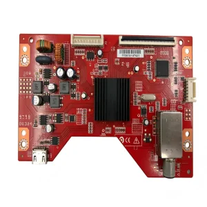
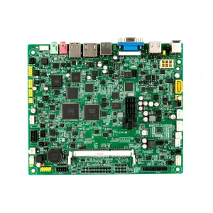
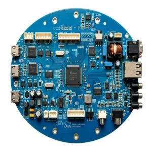
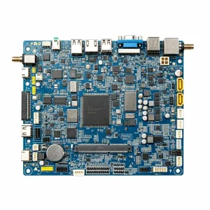
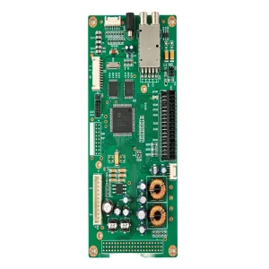
Demonstrating mission-critical electronics manufactured with zero-defect methodologies across green energy, industrial controls, and IoT ecosystems.
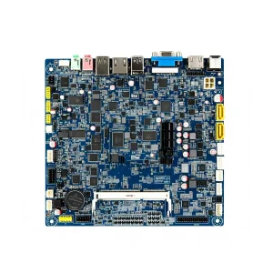

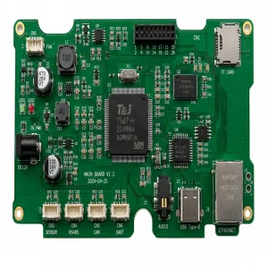
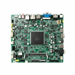
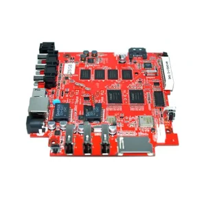
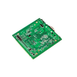
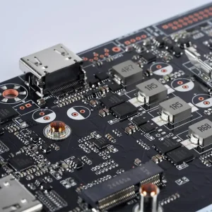
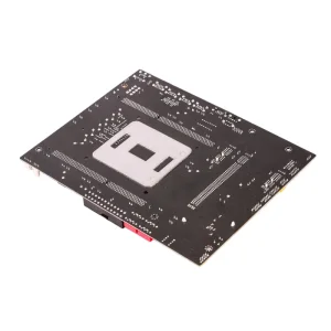
Strategic integration of bare fabrication, active/passive component pipelines, and high-throughput SMT processing provides an unmatched competitive matrix.
Shenzhen's Greater Bay Area houses the world's most concentrated semiconductor distribution and substrate fabrication facilities. Parts sourcing that takes weeks in Western markets executes in under 24 hours, dramatically compressing NPI (New Product Introduction) cycles.
Equipped with state-of-the-art Yamaha, Panasonic, and Fuji high-speed modular mounters capable of 01005 passives and 0.3mm pitch ultra-fine BGAs, our factory floor achieves placement accuracy reaching ±0.03mm under strict cleanroom conditions.
Integrated Manufacturing Execution Systems (MES) generate unique serialization tags for individual PCBA units. Real-time logging maps every solder paste height, thermal reflow profile, AOI result, and functional validation test to its source material batch.
Bridging the geographical divide with localized customer operations, stringent IP shielding, and internationally recognized process audits.
Every Gerber and Bill of Materials undergoes a 32-checkpoint Design for Manufacturability review before release, mitigating solder bridging, acid traps, and component clearance failures.
Complete confidentiality with binding NDA frameworks, separated R&D air-gapped programming networks, and strict floor-level surveillance preventing proprietary layout leakage.
Certified operational workflows aligned with IATF 16949 (Automotive), ISO 13485 (Medical), ISO 9001, and ISO 14001, ensuring full compliance with RoHS, REACH, and UL flammability standards.
Direct contact with experienced bilingual electronics engineers across US, European, and Asian business hours eliminates delivery bottlenecks and facilitates instant change orders (ECN).
Analyzing the balance between onshore agile design and offshore scalable volume manufacturing to optimize cost, lead times, and technological resilience.
Global enterprises increasingly deploy a "China + 1" approach or leverage Chinese OEM factories for rapid, low-friction volume ramps while preserving local domestic hubs for final mechanical assembly, drastically reducing landed unit cost.
The explosion of Edge AI and compact telematics requires micro-vias, stacked laser vias, and 0.4mm pitch CSP packaging. OEM factories with advanced automated optical and 3D X-ray inspection (AXI) have become indispensable partners.
Procurement teams demand more than bare PCBA. Forward-thinking OEMs deliver complete box-build integration: ultrasonic plastic welding, conformal coating, custom wire harnessing, and finished retail packaging delivered directly to global fulfillment centers.
Custom circuit manufacturing tailored to the extreme operating parameters of various demanding commercial sectors.
Under-the-hood microcontrollers and transmission units built with high-Tg FR-4, thick copper traces, and thermal potting to survive harsh vibrations and temperature extremes (-40°C to +125°C).
Class II/III medical circuit assemblies with low dielectric loss, exceptional signal-to-noise ratios, and comprehensive functional test fixtures that prevent diagnostic drift over years of clinical operation.
Photovoltaic and wind power inverter boards that manage high switching transients, featuring creepage and clearance routing that exceeds standard IEC safety limits to safeguard critical infrastructure.
Ultra-low quiescent current IoT sensor boards with nano-conformal coatings that prevent moisture-induced dendritic growth in subterranean and corrosive wastewater monitoring installations.
Key technical and logistical considerations for qualifying a high-reliability Chinese PCBA manufacturing partner.
Specialized builds addressing high-speed data acquisition, automotive control, and heavy industrial power systems.