Explore specialized sub-assemblies built under rigorous DFM and quality assurance protocols, serving enterprise networking, healthcare diagnostics, automotive steering, and intelligent automation systems.
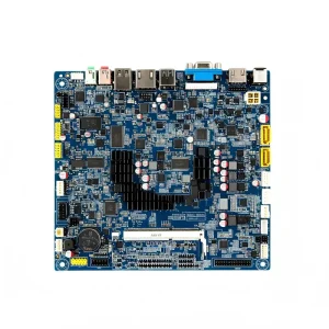
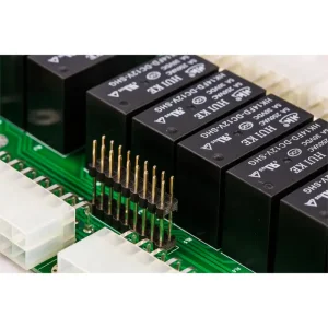
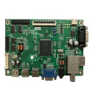
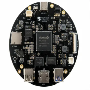
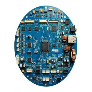

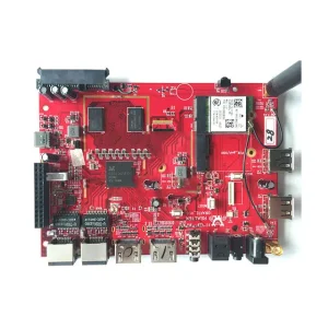
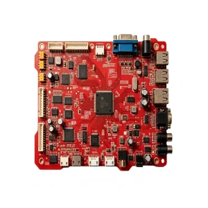
Modern electronic contract manufacturing has transitioned from simple component placement to multi-layered, highly integrated electro-mechanical engineering. OEM requirements demand unprecedented precision, thermal dissipation management, and ultra-dense interconnection capabilities.
As Internet-of-Things (IoT), smart wearables, and compact automotive compute modules advance, OEMs require circuit boards with micro-vias, stacked blind/buried vias, and pitch limits tightening below 0.35 mm. Manufacturing facilities must deploy high-speed, dual-beam placement platforms equipped with cognitive vision inspection to avert tombstoning, voiding, and micro-bridging.
Electrification in automotive powertrains (BMS, EPS), industrial motor drives, and gallium nitride (GaN) / silicon carbide (SiC) power supplies generate extreme watt-density footprints. Today's manufacturing requires metal-core PCBs (MCPCB), heavy-copper fabrication up to 6 oz, ceramic substrate assembly, and localized coin insertion to maintain heat dissipation stability.
Regulatory compliance authorities require end-to-end auditability. OEM buyers can no longer rely on unverified manual batch logs. Every raw capacitor, active IC, PCB panel, and solder paste paste cartridge must be bound to a unique 2D DataMatrix code tracked through automated Manufacturing Execution Systems (MES) and real-time ERP nodes.
Procurement leaders at Fortune 500 enterprises and hyper-growth scale-ups evaluate PCBA manufacturing partners through the multidimensional lens of component lifecycle stability, DFM-driven yield optimization, and intellectual property fortresses.
The global semiconductor landscape continues to experience cyclical allocation shortages. A single passive inductor or specialized MCU shortage can halt entire turnkey production lines. Top-tier OEM manufacturing requires programmatic Bill-of-Materials (BOM) health scoring during the engineering quote stage.
STHL maintains deep integrations with tier-1 authorized component distributors (Mouser, Digi-Key, Avnet, Arrow) combined with pre-qualified localized authorized distributors. Our dedicated procurement engineering division constantly provides pin-compatible and functional alternate suggestions, reducing lead-time risks from 36 weeks down to 4 weeks.
Early DFM / DFA Intervention: STHL's engineering review detects over 94% of potential manufacturing roadblocks—such as solder bridging risks, inadequate component clearances, and thermal balance mismatches—before raw copper laminates are engraved.
| Procurement Dimension | Traditional EMS Broker | STHL OEM Factory Model |
|---|---|---|
| Pricing Structure | Hidden middleman markups | Transparent Factory Direct |
| BOM Risk Audit | Reactive upon part failure | Proactive lifecycle & EOL scrub |
| Quality Ownership | Fragmented across sub-tiers | Single Accountable Entity |
| Minimum Order Qty | Rigid (e.g. 5,000+ pcs minimum) | No MOQ / Rapid Pilot to Scale |
| IP & NDA Protection | Informal paper agreements | Strict IP quarantine & digital vaults |
Different operational environments demand distinct material formulations, solder alloys, coating chemistries, and environmental stress screening. Explore our sector-specific turnkey competencies.
In-vehicle safety and powertrain systems operate under intense vibration, extreme temperature fluctuations (-40°C to +125°C), and chemical exposure. We build Supplemental Restraint Systems (SRS), Electric Power Steering (EPS), and Battery Management Systems (BMS) with Zero-Defect frameworks.
Biochemical analyzers, radiation detectors, and bedside physiological monitors necessitate unwavering precision and biocompatible cleanliness. Solder purity, ionic contamination resistance, and firmware serialization form the foundation of our healthcare assembly line.
Smart grid power supplies, uninterruptible power supplies (UPS), and sensor interface modules are designed to run 24/7/365 without failure. We integrate heavy copper traces, surge arrestors, optical isolation, and robust mechanical enclosures to survive high-EMC factory floors.
Quality is designed into the process, not merely inspected after assembly. Review our standard operational capability matrix configured for advanced surface mount technology.
| Manufacturing Stage | Hardware & Systems Deployed | Process Tolerances & Parameters | Quality Verification Gate |
|---|---|---|---|
| Pre-Engineering DFM | Valor Genesis / CAM350 Engineering Stations | Gerber, IPC-2581, ODB++, XY Data validation | Engineering Query (EQ) sign-off prior to PCB fab |
| Solder Paste Application | GKG High-Precision Fully-Auto Stencil Printers | Repeatability: ±10 µm; 0.3 mm pitch aperture fidelity | Inline 3D Koh Young SPI (Volume, Area, Coplanarity) |
| High-Speed SMT Placement | Yamaha YS24 / Fuji NXT Modular High-Speed Lines | Placement accuracy: ±0.025 mm (QFP, BGA, 01005) | Intelligent feeder optical barcode component verification |
| Thermal Soldering | JT 10-Zone Reflow with Pure N2 Atmosphere | Real-time KIC thermal profiling; peak temp control ±1.5°C | Continuous profile logger; dynamic atmosphere control |
| Optical & X-Ray Inspection | Mirtec 3D AOI & Seamark Automated 3D X-Ray (AXI) | Defect capture: bridging, tombstoning, head-in-pillow, voiding < 15% | 100% automated inspection with MES image archiving |
| THT Insertion & Soldering | Selective Soldering Systems & Lead-Free Wave Solder | Nitrogen hooded wave; customized titanium pallets | Visual IPC-A-610 Class 2/3 solder joint criteria |
| Functional Testing (FCT) | Customized Bed-of-Nails fixtures & Test Fixtures | CAN-bus, RF attenuation, voltage rail validation, LED luminescence | Pass/Fail automated serialization write to cloud database |
| Conformal Coating & Box Build | PVA Robotic Selective Dispensing System | Acrylic, silicone, polyurethane coatings; 50–150 µm thickness | UV blacklight illumination inspection; ingress leak testing |
Connecting manufacturing in Shenzhen with engineering teams across North America, Europe, and Asia-Pacific through uncompromised international standards, expedited customs routing, and real-time project management.
Global product distribution demands continuous adherence to RoHS 3 (EU 2015/863), REACH (SVHC declaration), and Halogen-Free directives. STHL maintains an internal XRF screening spectrometer to verify raw circuit boards and lead-free alloy solder bars before fabrication starts.
Shipping bare PCBA or integrated box-build units requires protective ESD packaging, vacuum-sealed anti-static barrier shielding, and custom silica gel desiccant packs. We provide turnkey DDP (Delivered Duty Paid), FOB, and DAP logistics to your fulfillment centers or manufacturing plants globally.
Proprietary algorithms and hardware schematics represent our clients' most valuable intellectual property. STHL enforces air-gapped programming stations, hardware security module (HSM) key flashing, and legally enforceable mutual non-disclosure agreements prior to RFQ document sharing.
To maintain an enduring competitive advantage, our manufacturing ecosystem continuously evolves to accommodate breakthroughs in edge AI computing, advanced heterogenous packaging, and environmentally sustainable materials.
Transitioning passive resistors and capacitors into inner PCB substrate layers to unlock up to 40% surface board space savings. Enabling hyper-dense edge compute platforms, advanced wearables, and multi-radio IoT sensor nodes.
Integrating artificial intelligence algorithms directly into 3D SPI and 3D AOI inspection stations. Dynamic feedback loops automatically recalibrate stencil wipe frequencies and placement head offset vectors in real-time, driving zero-defect thresholds.
Developing specialized production runs utilizing bismuth-tin low-temp solders (reflow peak < 175°C) to enable sensitive optics and biodegradable substrate assembly, dramatically slashing carbon footprint and thermal component warpage.
Get direct, authoritative answers to the primary commercial, manufacturing, and operational considerations when partnering with our turnkey assembly factory.
To provide a fully transparent, line-item turnkey quotation within 24–48 hours, our engineering team requires: (1) Complete Gerber files in RS-274X format or IPC-2581/ODB++ data including board outline and drill tables; (2) A consolidated Bill of Materials (BOM) in Excel format containing part references, quantities, manufacturer names, and complete manufacturer part numbers (MPN); (3) Pick-and-Place (Centroid) XY coordinate data; and (4) Any specialized testing, programming, or conformal coating instructions.
No, we enforce zero Minimum Order Quantity (MOQ). We support new product introductions (NPI) from rapid functional prototypes (1 to 5 boards) up to high-volume commercial production exceeding 500,000 units. Prototype batches are processed on identical high-precision SMT lines as mass production, guaranteeing that the thermal reflow and placement parameters established during pilot validation seamlessly scale to volume runs.
We operate a stringent Anti-Counterfeit Policy. All electronic components are procured exclusively through tier-1 franchised distributors or factory-direct manufacturers (e.g., Texas Instruments, STMicroelectronics, NXP, Analog Devices, Murata). Every incoming reel is verified through our Incoming Quality Control (IQC) laboratory, featuring decapsulation, marking permanency solvents, pin oxidation inspections, and XRF material analysis. Traceability is recorded in our MES down to the specific purchase order and lot number.
For rapid-turn prototype assemblies with pre-kitted parts, boards can be assembled and shipped in as fast as 24 to 48 hours. Turnkey prototype builds typically take 7 to 10 working days, subject to the procurement lead time of specific active ICs. Full-scale production cycles generally span 3 to 4 weeks for bare board fabrication, component sourcing, SMT/THT assembly, conformal coating, box-build integration, and end-of-line functional stress testing.
Every assembly featuring BGA, QFN, LGA, or CSP packages passes through our Automated 3D X-Ray Inspection (AXI) stations. Our high-resolution X-ray systems evaluate solder ball roundness, diameter, bridging, open circuits, and measure voiding percentages against IPC-A-610 Class 3 limits (which strictly cap solder voiding at less than 15% to 25% depending on critical thermal pad classifications).
Yes. We offer fully hybrid sourcing models. OEM customers may provide pre-programmed proprietary microcontrollers or specialized custom ASICs on consignment, while allowing our factory to procure standard passives, discrete diodes, power management ICs, and mechanical connectors. Our ERP system segregates and tracks customer-consigned materials with identical lot-level precision as our turnkey stock.
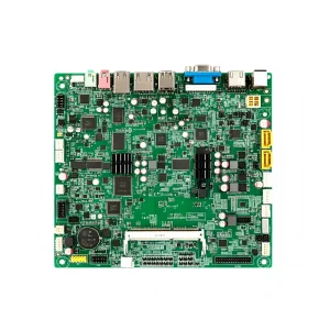
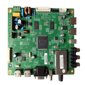
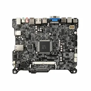
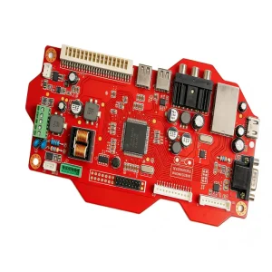
Review our specialized assemblies designed for nuclear radiation detection, high-voltage battery management systems, intelligent safety interlocks, and critical telemetry controllers.



Connect directly with our senior process engineers. Upload your Gerber files and BOM under mutual non-disclosure agreement for a complimentary DFM analysis and verified line-item quote.
