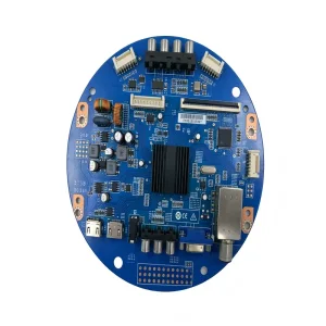
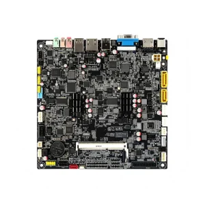
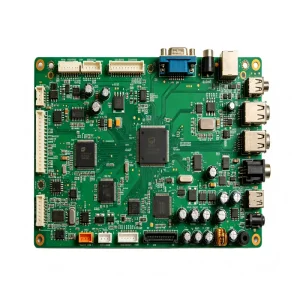
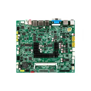
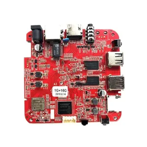
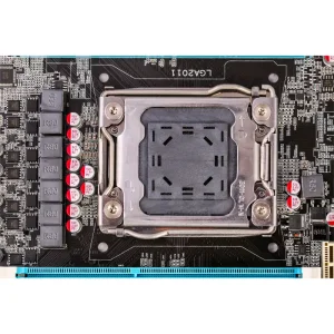
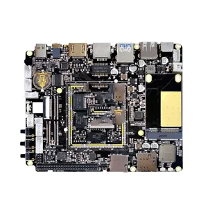
Direct factory turnkey assemblies tested to ISO 13485, IATF 16949, and EN standards. Explore our advanced mission-critical modules deployed across European industrial systems.

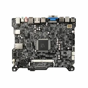
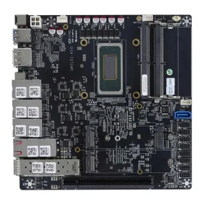
Across the European Union and the broader EMEA economic theater, the electronics manufacturing ecosystem is navigating profound structural realignment. Emerging regulatory pressures, accelerated transition toward Industry 5.0, rising geopolitical instability, and ambitious green transitions under the European Green Deal have challenged traditional OEM procurement paradigms. Modern European hardware innovators—ranging from German automotive Tier-1 engineering centers and Nordic MedTech clusters to Italian industrial robotics specialists—face complex operational equations. While the concept of local nearshoring within Central and Eastern Europe (CEE) has gained political visibility, persistent supply chain choke points, elevated structural energy tariffs, severe qualified labor constraints, and limited raw silicon substrate availability have illuminated the real economic boundaries of purely localized production.
Consequently, forward-looking procurement leaders and Chief Technology Officers throughout the EU are embracing high-efficiency hybrid electronics manufacturing strategies. In this optimized paradigm, European R&D divisions concentrate their resources on advanced intellectual property creation, architectural embedded systems design, high-level functional safety validations, and firmware security. Simultaneously, physical manufacturing execution—spanning complex multilayer printed circuit board fabrication, high-speed Surface Mount Technology (SMT), automated Through-Hole Technology (THT/DIP), and complete box-build integration—is executed in direct collaboration with digitalized, Industry 4.0 Chinese smart factories possessing unparalleled component liquidity and agile production capacity.
Operating an OEM PCB assembly supply chain serving European enterprises requires absolute synchronization with mandatory European Union directives and harmonized standards. Failure at the compliance verification stage leads to catastrophic product seizures, market recalls, and severe financial penalties under the EU Market Surveillance Regulation. Precision manufacturing for the EU territory requires uncompromising operational mastery over:
• CE Marking and Electromagnetic Compatibility (EMC Directive 2014/30/EU): Ensuring that dense, high-frequency layouts minimize unwanted radiated emissions and maintain robust immunity against industrial electrostatic discharges (ESD) and conducted electrical fast transients (EFT). This demands strict Design for Electromagnetic Compatibility (DF-EMC) protocols during PCB stackup engineering and ground plane segmentation.
• RoHS Directive 2011/65/EU and Delegated Directive (EU) 2015/863 (RoHS 3): Complete elimination and quantitative lab verification of hazardous substances, specifically lead (Pb), cadmium (Cd), mercury (Hg), hexavalent chromium (Cr6+), and specific phthalates (DEHP, BBP, DBP, DIBP). Precision reflow profiles must be calibrated specifically for lead-free solder alloys such as SAC305 (Sn96.5Ag3.0Cu0.5) with narrow peak process windows (235°C to 245°C) without damaging sensitive thermal packaging.
• REACH Regulation (EC No 1907/2006): Continual auditing of Substances of Very High Concern (SVHC) across all passive, active, and electromechanical components, solder flux chemistry, and conformal coating solvents to guarantee compliance with the rolling candidate list published by the European Chemicals Agency (ECHA).
• WEEE Directive 2012/19/EU: Implementation of Design for Disassembly (DfD) guidelines, allowing European recyclers and end-users to cleanly segregate hazardous electronic assemblies, lithium-ion battery packs, and metallic sub-assemblies at the end of product life cycles.
Evaluating the operational trade-offs between localized Western European assembly houses, nearshore Eastern European contractors, and modern turnkey Industry 4.0 Chinese manufacturing facilities:
| Operational Dimension | Western European EMS | Nearshore CEE Facilities | China Industry 4.0 (STHL Model) |
|---|---|---|---|
| Component Access & Liquidity | Limited local buffer; dependent on global distributors with 16-26 week lead times. | Moderate buffer; recurring shortages for specialized passive arrays and ASICs. | Unmatched component cluster: direct access to 500k+ qualified MPNs and primary distributor hubs. |
| SMT Line Reconfigurability | High setup overheads; strict MOQ thresholds; costly changeovers for low-volume runs. | Moderate agility; focused heavily on repetitive mid-to-high volume automotive runs. | Zero MOQ friction; seamless NPI-to-mass-production transition on identical SMT/AOI lines. |
| Prototyping & DFM Feedback | 5 to 10 working days; thorough but slower engineering cadence. | 4 to 7 working days; variable DFM automation depth. | 24-48 hour comprehensive DFM/DFA turnaround; automated stackup and footprint impedance simulation. |
| Tooling & Setup Expenditure | Premium cost structure driven by regional labor overhead and high utility tariffs. | Competitive tooling; rising wage inflation and utility cost indexing. | Lean tooling structure with optimized amortized stencils, fixtures, and automated test rigs. |
| Traceability & MES Integration | Comprehensive ERP systems; high compliance cost reflected in customer pricing. | Standard compliance tracking; variable granular board-level unit tracing. | Full 2D matrix barcode laser-marked trace: solder paste volume, pick-and-place nozzle, AOI/X-ray log. |
Why modern turnkey manufacturing in Shenzhen outperforms fragmented regional sourcing through digitalized MES integration, automated optical inspection, and localized electronic component ecosystems.
State-of-the-art modular surface mount lines utilizing 3D SPI (Solder Paste Inspection) systems evaluate paste deposit height, area, and volumetric uniformity prior to component placement, mitigating 70% of potential assembly anomalies at zero stage.
High-resolution inline 3D AOI (Automated Optical Inspection) combined with closed-tube high-magnification oblique X-ray inspection inspects hidden solder joints on Ball Grid Arrays (BGA), Quad Flat No-leads (QFN), and ultra-dense 01005 passive chips.
Every printed circuit board receives an individual high-density laser-etched DataMatrix 2D code. The MES (Manufacturing Execution System) continuously binds component lot numbers, feeder position, reflow oven temperature profiles, and operator IDs.
Engineered to conquer harsh operating environments, stringent functional safety requirements, and prolonged operational lifecycles.
Strictly conforming to IATF 16949 standards. High-voltage insulation barrier control, heavy copper busbar soldering, and resilient potting for on-board vehicle control units, inverter gate drivers, and EV chargers serving the German and Nordic automotive corridors.
Certified to ISO 13485 quality protocols. Ultra-clean assembly, bio-compatible conformal coating, and full component lot validation for diagnostic ultrasound gear, surgical visualization cards, and portable monitoring sensors across Swiss and Benelux medtech hubs.
High-vibration resistant DIP pinning, selective automated wave soldering, and automated conformal coating to resist corrosive atmospheres, micro-dust, and thermal spikes in European robotic cells, PLC platforms, and intelligent distributed servo drives.
Heavy-copper PCBA architectures (up to 6oz outer/inner copper) designed for sustained high thermal dissipation and current saturation in decentralized renewable microgrid inverters and commercial battery storage installations across Southern and Western Europe.
True engineering excellence in OEM PCB assembly is achieved not by post-production screening, but through rigorous process capability controls implemented at every phase of physical assembly. Modern high-reliability electronics demand zero-defect tolerance (PPM < 10), particularly when boards are permanently encapsulated in resin or installed in inaccessible subsea, remote wind farm, or automotive environments.
Before copper is etched or solder stencils are laser-cut, our engineering team subjects the client's complete Gerber, ODB++, and BOM documentation to exhaustive Design for Manufacturability (DFM) and Design for Assembly (DFA) audits. We analyze trace clearance down to 3mil, assess thermal relief on massive power ground planes, verify BGA escape routing, and cross-reference component land patterns against IPC-7351 guidelines. Discrepancies between centroid data, solder mask openings, and physical reel package outlines are caught and rectified in writing within 24 to 48 hours, eliminating costly redesign loops during pre-production pilot runs.
In accordance with IPC-A-610 Class 3 specifications, our reflow ovens operate with 10 to 12 closed-loop temperature zones and inert nitrogen (N2) atmosphere injection. Controlling oxygen saturation below 500 PPM prevents oxidation of fine-pitch lead surfaces, ensures pristine intermetallic compound (IMC) thickness (1 to 3 microns), and virtually eliminates micro-voiding within high-pin-count BGA solder spheres. For mixed-technology boards incorporating high-mass transformers, inductors, and connectors, programmable selective soldering systems apply targeted flux and localized nitrogen-shielded solder waves, protecting adjacent heat-sensitive surface mount passives from extreme thermal shock.
Physical assembly constitutes only part of the manufacturing equation; validation confirms device integrity. We engineer custom modular FCT test jigs featuring pneumatically actuated bed-of-nails fixtures that interface with client firmware via JTAG, SWD, or UART interfaces. Automated test software scripts exercise on-board voltage regulators, signal buses, RF transceivers, and digital I/O lines under simulated full electrical load. When required for harsh automotive or offshore renewable applications, assemblies undergo Burn-In environmental stress screening, thermal shock cycling (-40°C to +125°C), and damp-heat endurance testing (85°C / 85% RH) to trigger and eliminate infant mortality failures before dispatch.
Detailed technical answers for European procurement managers, quality auditors, and chief hardware architects.
Complementing our core power and automotive assemblies with smart sensors, high-speed networking, medical CT, and optoelectronic solutions engineered for global commercial distribution.
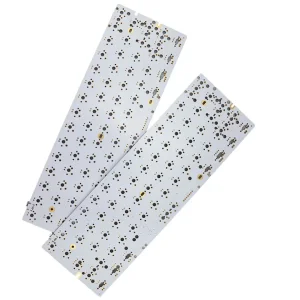
Quantitative technical capabilities supporting advanced European electronics manufacturing requirements.
Standard FR-4 (Tg 150°C to 180°C), High-frequency Rogers / Taconic, Polyimide Flex, Rigid-Flex, Metal Core Aluminum (1.0 to 3.0 W/m-K), Ceramic substrates, Halogen-free laminates.
Passives down to 01005 (0402 metric) chips, Ultra-fine pitch 0.35mm BGA/micro-BGA, QFN/DFN, Pop (Package on Package), WLCSP, Connectors up to 150mm length with optical lead coplanarity checks.
Lead-Free HASL, Electroless Nickel Immersion Gold (ENIG), Immersion Silver, Immersion Tin, OSP, ENEPIG (Electroless Nickel Electroless Palladium Immersion Gold) for wire bonding.
Custom aluminum CNC milling, plastic injection housing tool development, ultrasonic plastic welding, silicone seal dispensing, cable wire harness assembly, laser serial marking, custom retail packaging.