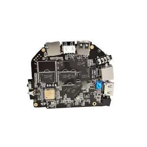
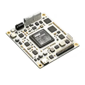
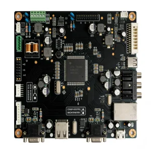
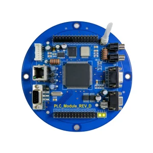
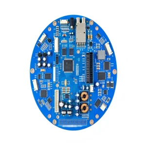
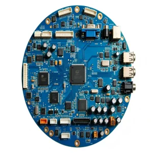
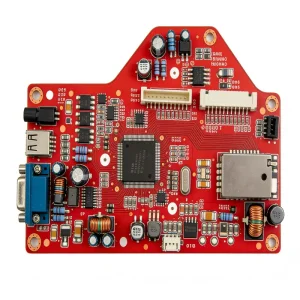
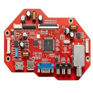
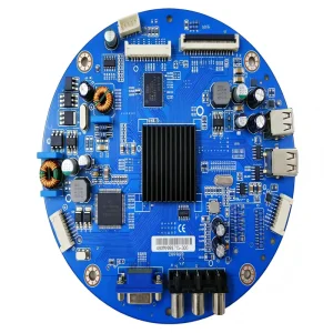
Explore specialized industrial, automotive, and medical PCBA modules manufactured under strict IPC-A-610 Class 3 specifications.
Strategic transformations shaping modern Original Equipment Manufacturer (OEM) PCB Assembly ecosystems globally.
The electronics industry has shifted from pure offshore cost-reduction toward resilient multi-tier sourcing. Global tier-1 OEMs require integrated supply chains capable of quick-turn NPI and scalable mass manufacturing with dual-source BOM security to mitigate cross-border geopolitical and logistic disruption risks.
Micro-miniaturization, 5G RF front-ends, and edge AI hardware require 01005 component mounting and 0.35mm pitch BGA placement. OEMs demand manufacturing partners with smart reflow profiling and automated optical verification to achieve zero-defect assembly across 30+ layer rigid-flex configurations.
Standard quality verification is no longer sufficient. Enterprise automotive and mission-critical electronics require MES-level lot tracking, linking every discrete passive, IC lot, and reflow profile matrix directly to unique unit barcodes for auditable component-level traceability.
Comprehensive technical benchmarks, tolerances, and inspection protocols maintained in our production facility.
| Manufacturing Dimension | Process Engineering Standard | Technical Threshold / Equipment Spec |
|---|---|---|
| Surface Mount Technology (SMT) | High-Speed Modular Pick-and-Place | Pitch down to 0.3mm; Chip placement down to 01005 & 0201 packages; ±0.03mm precision. |
| BGA & Advanced Packages | Ultra-Fine Pitch Placement & Rework | Micro-BGA, PoP (Package-on-Package), QFN, CSP; Pitch down to 0.35mm with nitrogen reflow option. |
| Through-Hole (THT / DIP) | Automated & Manual Wave Soldering | Selective wave soldering, RoHS lead-free solder pot alloy verification, IPC Class 2 and Class 3 fillets. |
| Quality Verification | In-Line Automated Optical & Radiographic | 3D SPI (Solder Paste Inspection), 3D AOI, 2D/3D Industrial X-ray inspection for BGA voiding <10%. |
| Value-Add Post Assembly | Protection & Environmental Hardening | Robotic conformal coating (acrylic, polyurethane, silicone), UV curing, potting, ultrasonic welding. |
| Board Substrate Compatibility | Multilayer Rigid, Flex, Rigid-Flex, IMS | Standard FR-4, High-Tg, Rogers RF, Polyimide Flex, Heavy Copper (up to 12oz), Aluminum MCPCB. |
Meeting regional certification protocols across North America, the European Union, and Asia-Pacific markets.
Complete assembly conformance with UL 796 flammability ratings, FCC Part 15 Class A/B EMI suppression protocols, and ANSI/ESD S20.20 certified cleanrooms. Full support for ITAR-sensitive commercial designs via strict data isolation and secure NDA protocols.
Strict supply-chain qualification guaranteeing 100% RoHS 3 (Directive 2015/863) and REACH compliance. Integration of lead-free SAC305/SN100C solder alloys, WEEE-aligned recyclable packaging, and technical construction files (TCF) for seamless CE marking.
Audited production environments compliant with IATF 16949 for automotive PPAP level 3 submissions, including IMDS reporting. Dedicated ISO 13485 medical device lines with Device History Record (DHR) generation and static process validation protocols.
Proven execution across specialized deployment scenarios requiring enhanced durability and reliability.
Our ECU and BCM solutions feature AEC-Q200 passive components, automated potting, and conformal coating to withstand -40°C to +125°C thermal cycling, high-vibration engine bay dynamics, and surge dump transients.
Class III medical assemblies manufactured under strict particulate limits. Precision impedance matching (±5%), low-leakage current verification, and 100% ICT (In-Circuit Testing) ensure uncompromised clinical signal integrity.
Isolated DC-DC power converters and multi-sensor water quality analyzers built with thick-copper PCB technology, thermal via arrays, and specialized potting for extended service lives exceeding 100,000 hours MTBF.
Continuous investment in artificial intelligence, advanced materials, and environmental electronics assembly.
Engineering and procurement specifics answered by our senior technical staff.
Our engineering team performs a multi-point Design for Manufacturability (DFM) and Design for Assembly (DFA) audit before cutting stencils. We cross-verify component pad footprints against actual package geometries, evaluate thermal relief paths, verify component clearances for automated nozzle access, and assess component pin-to-pad ratios, preventing costly board re-spins.
We source directly from original component manufacturers (OCM) and authorized global distributors (including Arrow, Avnet, Digi-Key, Mouser). All non-franchised spot buys undergo incoming QA verification in our testing lab, including decap analysis, microscopic marking verification, solderability testing, and XRF material analysis.
Yes. Our manufacturing floors feature fully automated SMT lines alongside selective wave soldering, robotic point-to-point soldering, and precision servo-controlled press-fit machines equipped with real-time force-displacement monitoring to eliminate PCB substrate cracking during connector insertion.
We utilize multi-axis 3D X-ray inspection systems (AXI) calibrated to measure solder voiding percentages, bridging, head-in-pillow (HiP) anomalies, and wetting angles on non-visible terminations. Every critical BGA placement is monitored against IPC Class 3 voiding thresholds (<15% total voiding).
Beyond automated optical and in-circuit testing (ICT), we design customized Functional Test (FCT) jigs, perform firmware flashing, and conduct environmental stress screening (ESS), including thermal shock (-40°C to +125°C), high-humidity burn-in, and frequency-swept vibration testing prior to carton packing.
To deliver an itemized quotation within 24 hours, we require ODB++ or RS-274X Gerber data, an Excel BOM complete with manufacturer part numbers (MPN), approved alternate manufacturers, reference designators, centroid (pick-and-place XY data), and test specifications or functional test guidelines.
Turnkey electronic assemblies spanning telecommunications, consumer electronics, and computing infrastructure.