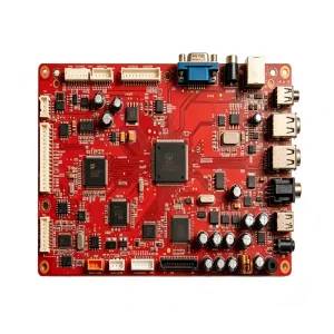
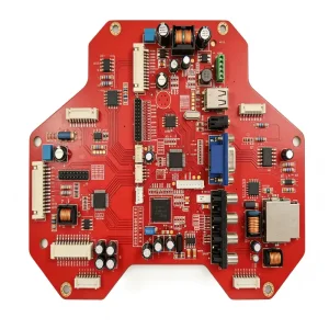
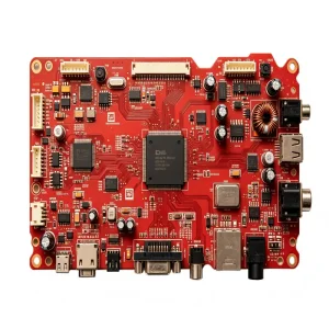
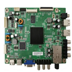
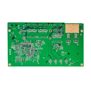
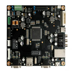
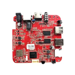
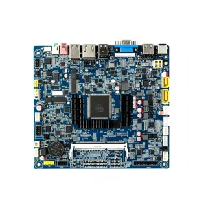
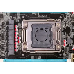
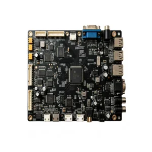
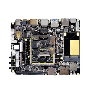
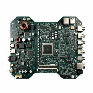
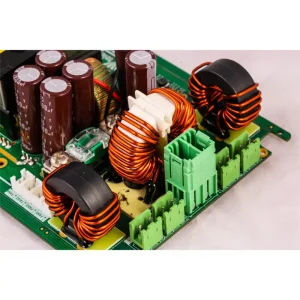
Engineered to exact IPC Class 2/3 specifications, our assembly capabilities span automotive telematics, high-frequency RF networks, and high-density industrial control systems.
The shifting dynamics of global electronics assembly require unprecedented levels of thermal optimization, component miniaturization, and end-to-end provenance verification.
Modern hardware architectures demand ultra-fine pitch ball-grid arrays (BGA down to 0.3mm pitch) and 01005 micro-passives. Advanced OEM manufacturing lines utilize real-time optical closed-loop solder paste inspection (SPI) to eliminate solder bridging and tombstoning at inception.
With the mass adoption of Gallium Nitride (GaN) and Silicon Carbide (SiC) switching devices in automotive and energy sectors, SMT engineering must accommodate high dV/dt transient responses and critical thermal dissipation requirements via specialized heavy copper and IMS substrates.
Geopolitical vulnerabilities mandate multi-tier obsolescence tracking. Through strict OCM (Original Component Manufacturer) and authorized franchise partnerships, component engineering verifies die markers, decapsulation integrity, and humidity-sensitive packaging standards.
Bridging the operational divide between Tier-1 engineering requirements and high-velocity factory execution.
| Procurement Challenge | Systemic Risk Point | Factory OEM Solution | Engineering Benefit |
|---|---|---|---|
| Uncertain Component Lead Times | Production stoppages due to extended lead times on MCUs, PMICs, or passives. | BOM Cross-Referencing & Direct Factory Stock Sourcing via 100+ Authorized Channels. | Up to 40% reduction in procurement lead cycles without redesigning core board schematics. |
| Hidden Assembly Joint Flaws | Micro-voids under QFNs, BGAs, and LGA pads leading to field failure under thermal vibration. | Automated 3D In-Line Solder Paste Inspection (SPI) & High-Definition 3D X-Ray (AXI). | Sub-ppm defect rates with verifiable digital X-ray inspection logs tied to batch MES. |
| BOM Price Volatility | Unpredictable margin erosion due to fluctuating spot markets for active semiconductors. | Early Design-for-Procurement (DFP) optimization and bulk strategic allocation models. | Guaranteed cost-down roadmaps and stable volume pricing across multi-year product runs. |
| Environmental & Thermal Stress | Premature failure in harsh automotive, industrial, and outdoor telemetry deployments. | Robotic Selective Conformal Coating, Underfill Dispensing, and In-House Potting Lines. | IPC-CC-830 certified moisture, chemical, and thermal cycle isolation for 10+ year MTBF. |
From mission-critical medical diagnostics to harsh automotive thermal environments, our manufacturing infrastructure is tuned for uncompromising reliability.
Operating strictly within IATF 16949 parameters, assemblies undergo extensive Thermal Shock Testing (-40°C to +125°C), PPAP Level 3 documentation, and automated optical validation for in-cabin systems, T-Box interfaces, and EV battery management controllers.
Under ISO 13485 oversight, production takes place in controlled ESD environments. Every work order features component-level MES tracing, bio-compatible wash processes, and complete electrical functional testing for patient-connected hardware and diagnostic scanners.
Dedicated SMT workflows for high-frequency low-loss materials (Rogers, Megtron 6). Controlled impedance modeling within ±5% tolerance, microvia filling, and gold surface finishes (ENIG, ENEPIG) safeguard high-speed data integrity across switches and transceivers.
Complete supply chain integrity certified by international auditing bodies and supported by global engineering collaboration.
Our facility holds verified IATF 16949 (Automotive), ISO 13485 (Medical Devices), ISO 9001 (Quality), and ISO 14001 (Environmental) certifications. Every board undergoes strict Statistical Process Control (SPC) throughout fabrication and assembly.
Individual barcode matrix tracking links each placed passive or active IC to incoming supplier lot codes, pick-and-place nozzle telemetry, and final functional test parameters—providing ironclad traceability for global recalls or compliance audits.
Standard mutual Non-Disclosure Agreements (NDAs) govern all client technical data. Schematic diagrams, Gerber geometries, firmware, and test routines reside within isolated on-premise encrypted servers accessible only to cleared engineering personnel.
Continual capital investment in cutting-edge assembly hardware, smart manufacturing automation, and advanced substrate technologies.
Integration of deep-learning algorithms into 3D optical inspection to reduce false calls while boosting flaw identification in fine-pitch 0.3mm micro-BGAs.
Embedding resistors and capacitors directly into the inner dielectric layers of PCBs to clear outer surface area for ultra-compact IoT and wearable hardware.
System-in-Package (SiP) assembly incorporating multiple bare silicon dies, silicon interposers, and MEMS sensors on high-density organic substrates.
Complete lifecycle traceability with certified low-temperature solder alloys, closed-loop DI water reclamation, and solar-supported cleanroom environments.
Direct answers from our senior engineering team to assist hardware designers and global procurement leaders.
We procure 100% of electronic components from Original Component Manufacturers (OCMs) or their tier-1 authorized distributors (e.g., Digi-Key, Mouser, Arrow, Avnet). Factory inspection involves barcode verification, lot serialization, moisture-barrier checks, and internal lab testing when required.
Before running stencils or releasing fabrication files, our 50+ person engineering division conducts thorough DFM/DFA reviews. We analyze footprint pad geometries, component clear-space, thermal relief vias, solder mask slivers, and pick-and-place nozzle clearances to prevent assembly defects.
Yes. Our production floor operates 7 automated SMT lines paired with dual selective-wave soldering and semi-automated DIP through-hole insertion stations. We comfortably handle double-sided fine-pitch BGAs alongside high-power heavy copper through-hole connectors and press-fit pins.
Beyond standard AOI and 3D X-Ray, we engineer custom In-Circuit Test (ICT) bed-of-nails fixtures, run customer-specific functional firmware flash routines, execute Flying Probe tests for quick-turn validation, and support thermal cycling, burn-in chambers, and drop testing.
Discover our specialized high-performance board assemblies tailored for networking, medical diagnostics, enterprise computing, and clean power storage.