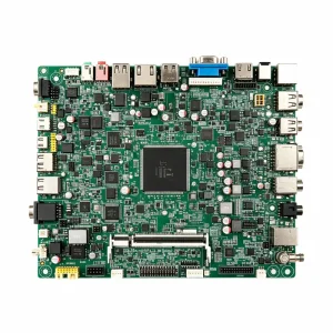
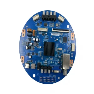
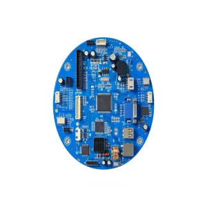
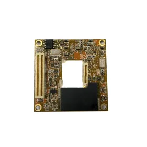
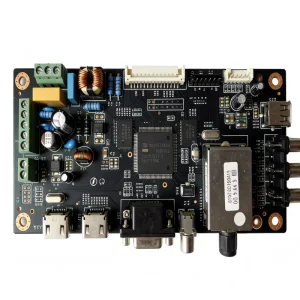
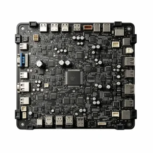
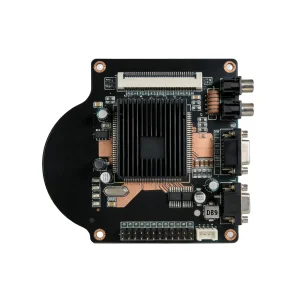
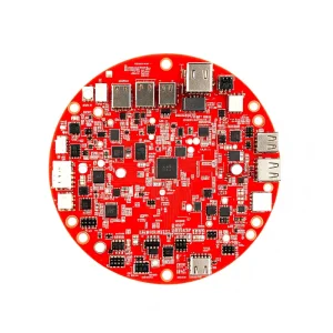
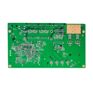
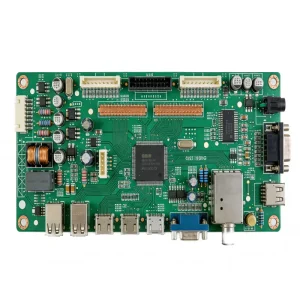
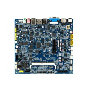
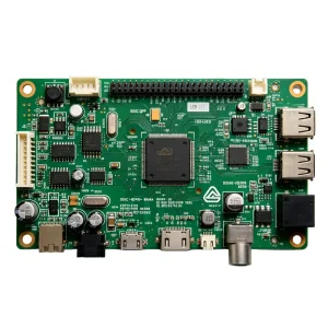
Engineered to automotive, aerospace, telecom, and industrial grade specifications. Explore our active turnkey manufacturing configurations.
In modern industrial electronics, the OEM PCB control board is no longer just a passive interconnect platform—it is the mission-critical epicenter governing power conversion, telemetry, computing, and electromechanical control. From automated factory floors to safety-critical automotive systems and mission-critical smart grids, system engineers demand sub-micron component placement accuracy, zero-defect solder integrity, and unbroken component traceability across every production lot.
The global demand for customized control boards is expanding exponentially, driven by electrification, edge computing, renewable energy storage, and industrial automation. Today's commercial infrastructure requires control assemblies capable of sustaining harsh operational parameters: extreme thermal cycling, prolonged electromagnetic interference (EMI), mechanical shock, and corrosive ambient environments. To meet these demands, top-tier OEM factories have transitioned from manual labor-intensive shops to fully automated, dust-free smart factories powered by Industry 4.0 data feedback loops.
While design teams in North America and Europe excel at system architecture and intellectual property development, China—specifically the Greater Bay Area and Shenzhen—remains the global epicenter for rapid-turn, high-density electronics manufacturing. This dominance is grounded in three undeniable operational pillars:
Turnkey OEM PCB control boards serve distinct regional and industrial profiles:
Empirical metrics reflecting 20 years of continuous turnkey EMS deployment and process refinement.
From component verification to box-build packaging, our end-to-end lines minimize handoffs and eliminate cross-vendor risks.
Dual-lane, high-speed SMT lines handling 01005 chips, 0.3mm pitch BGAs, POP technology, and wave-soldered through-hole assemblies with ease.
Certified to IATF 16949 (automotive), ISO 13485 (medical), ISO 9001, and ISO 14001 with comprehensive MES traceability across every single board.
Global component sourcing network accessing 500,000+ parts with authorized distributor relationships to mitigate obsolescence and supply chain shocks.
Integrated 3D SPI, automated optical inspection, 3D X-ray inspection for hidden ball grid joints, in-circuit testing (ICT), and full functional burn-in test beds.
How forward-thinking procurement teams select, audit, and scale with manufacturing partners in a complex semiconductor landscape.
Global procurement teams prioritize dual-sourcing architectures. OEM partners must deliver transparent second-source component suggestions with Pin-to-Pin compatibility without compromising electrical validation.
Rising bill-of-materials costs compel OEM buyers to lean on factory engineers for early DFM review—optimizing layer stack-ups, reducing solder pass requirements, and selecting efficient surface finishes like ENIG or OSP.
Strict Non-Disclosure Agreements (NDAs), network-isolated testing rooms, and encrypted firmware flashing routines ensure client proprietary code and architectural layouts remain fully protected during production.
Complete product assemblies manufactured under clean-room conditions with rigorous quality protocols.
Detailed technical, compliance, and procedural answers for procurement officers and engineering leads.