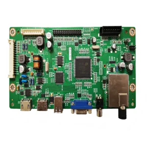
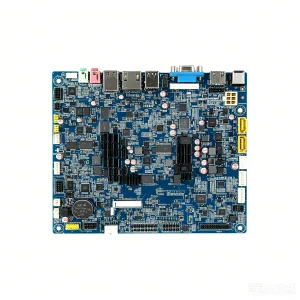
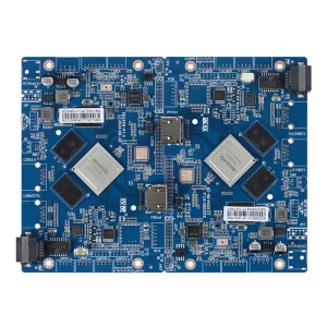
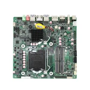
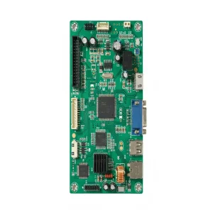
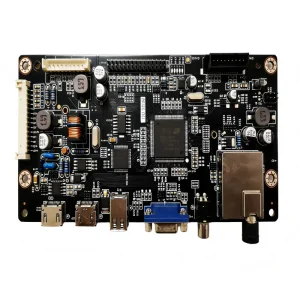
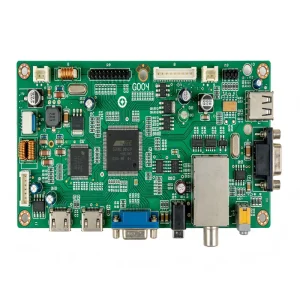
Explore real-world industrial deployments developed across our integrated surface-mount and substrate fabrication lines.
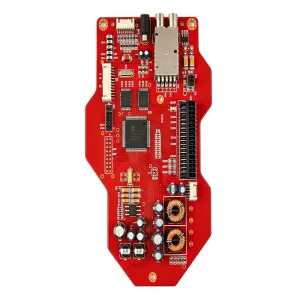
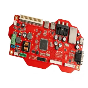
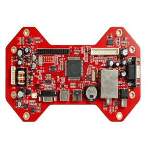

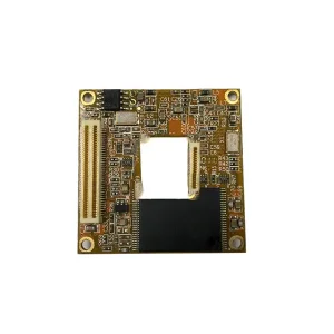


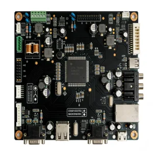
Analyzing supply chain migrations, multi-layer HDI transitions, and the demand for consolidated manufacturing.
Global original equipment manufacturers (OEMs) increasingly rely on integrated smart hubs capable of mitigating supply vulnerabilities. By uniting bare board production and component placement under centralized ERP/MES systems, manufacturers eliminate multi-tier handoffs, tariff discrepancies, and logistical lead-time delays.
The traditional dichotomy of sourcing bare substrates from one fabricator and sending them to an external SMT assembler introduces compound failure points. Consolidated OEM operations dramatically lower total landed costs by leveraging unified engineering reviews, panelization optimizations, and volume component acquisition.
Mission-critical electronics demand component-level lot tracing. With integrated MES infrastructure, automated pick-and-place systems log reel origin, reflow thermal profiles, and AOI inspection imagery per board serial number, satisfying stringent automotive (IATF 16949) and medical (ISO 13485) regulatory audits.
Continuous process improvements supported by fully synchronized SMT, DIP, and functional testing cells.
Precision-tailored electronic assemblies designed to withstand severe thermal, electromagnetic, and mechanical environments.
Demanding zero-defect manufacturing, autopilot compute nodes and sensor hubs rely on rigid-flex substrates, heavy-copper power distributions, and automated selective soldering to withstand engine compartment thermal cycles and road vibration profiles.
Medical instruments require absolute impedance control, ultra-low leakage currents, and biocompatible surface finishes. Assembly operations are conducted within particulate-controlled cleanrooms utilizing Class 3 soldering tolerances.
Utility-scale battery management systems (BMS) require high-voltage isolation, thick-copper thermal relief, and high-dielectric-strength FR4 variants. Integrated automated optical inspection (AOI) prevents cold solder joints under severe load.
Compact, high-density interconnections (HDI) paired with 0201 passives and 0.35mm pitch fine-pitch ball grid arrays (BGA). Solutions emphasize cost-effective automated high-speed mounting combined with integrated RF shield can placement.
Systematic capability benchmarks established across bare-board fabrication and automated assembly lines.
| Capability Parameter | Standard Production Tier | Advanced / High-Density Tier | Next-Generation Deployment |
|---|---|---|---|
| Layer Count | 1 - 16 Layers (Rigid FR4) | 18 - 32 Layers (Blind/Buried Vias) | Up to 48 Layers / Any-Layer HDI |
| Min. Line Width / Spacing | 3.5 mil / 3.5 mil (89 µm) | 2.5 mil / 2.5 mil (63 µm) | 1.8 mil / 1.8 mil (mSAP Process) |
| Component Packaging Range | 0402, QFP, standard SOP | 0201, 01005, 0.4mm pitch BGA | 03015 passives, 0.3mm ultra-fine BGA |
| Substrate Variances | FR-4 (Tg 130-170°C), CEM-3 | Rogers, Aluminum, Polyimide Flex | Ceramic (Al2O3/AlN), PTFE Hybrids |
| Surface Finishes | HASL, Lead-free HASL, OSP | ENIG (Immersion Gold), ENEPIG | Immersion Silver/Tin, Hard Gold Plating |
| Inspection Verification | Manual visual, standard 2D AOI | Inline 3D SPI, 3D AOI, 2D X-Ray | Inline 3D AXI (CT Slice-scan) |
Continuous process enhancement aligning with next-generation high-frequency, power-dense electronics.
Integration of real-time solder paste inspection (SPI) data feedback to screen printing machinery, reducing stencil-offset solder bridges and solder-volume defects prior to placement.
Transitioning beyond subtractive etching towards modified semi-additive processing (mSAP) to support fine-line RF architectures and embedded passive/active substrate integration.
Adoption of vacuum-assisted reflow soldering systems eliminating BGA voids below 5%, paired with water-soluble low-VOC flux variants and halogen-free substrate matrices.
Detailed engineering responses addressing common procurement, quality, and technical fabrication questions.
Turnkey manufacturing links the BOM scrubbing phase directly with authorized global distributor inventories. Engineering teams conduct immediate lifecycle analyses (checking EOL and LTB notifications) and recommend footprint-compatible pin-to-pin alternates during the Design for Manufacturability (DFM) stage, preserving the production schedule without re-spinning the layout.
Production runs default to IPC-A-610 Class 2 for standard commercial and industrial products, governing component alignment, solder wetting, and voiding thresholds. For automotive, aerospace, or medical deployments, operations adhere to IPC-A-610 Class 3 / IPC J-STD-001 requirements, incorporating comprehensive 3D X-ray inspection for bottom-terminated components (QFN/BGA).
Fabrication tolerances are monitored through controlled-dielectric layering and coupon-based time-domain reflectometry (TDR) measurements. Impedance tolerances (single-ended 50Ω, differential 90/100Ω) are held within ±5% to ±10% tolerances using laser direct imaging (LDI) for precise copper-width definition on high-speed layers.
All active integrated circuits are handled strictly under IPC/JEDEC J-STD-033 standards. Components classified above MSL Level 2 are stored within automated nitrogen desiccant dry cabinets (<5% RH). Should floor life exposure be exceeded, baking chambers are deployed under calibrated thermal profiles prior to automated surface mount placement.
Continuous volume shipments produced across consumer, IoT, and high-reliability industrial domains.