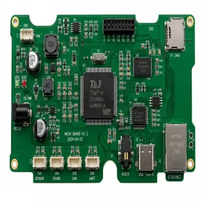
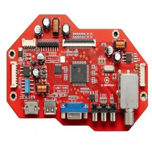
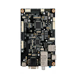
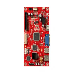
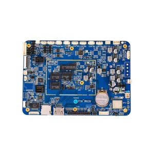

Ultra-High Density Interconnect (HDI)
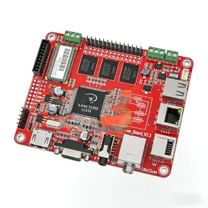
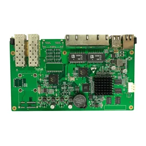
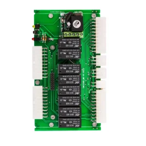
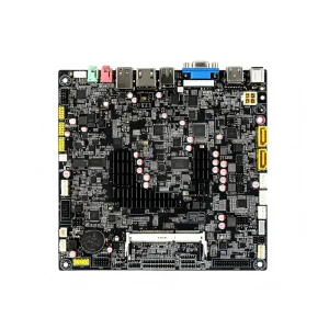
Modern microprocessors and system-on-chips demand trace geometries below 50µm/50µm line/space rules. OEM PCB fab manufacturers are shifting from traditional microvias to advanced Any-Layer HDI and Substrate-like PCB (mSAP) processes, enabling dense routing for compact enterprise devices without cross-talk or impedance mismatches.