Explore production-tested OEM PCB and PCBA solutions produced under IATF 16949 & ISO 13485 manufacturing controls.
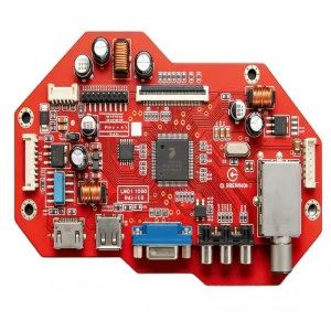


A granular breakdown of variables shaping electronic manufacturing costs, panel utilization yields, and layer-stack cost optimization.
The core substrate choices—ranging from high-Tg standard FR-4 (Tg 170°C+) to high-frequency polytetrafluoroethylene (Rogers RO4350B, RO4003C) and polyimide flex films—dictate raw baseline expense. Sourcing engineers must balance Dk/Df losses versus fabrication cost multiples.
A critical quotation variance driver is panel utilization percentage. By optimizing unit step-and-repeat arrays, breakout rails, fiducials, and tooling hole placement, smart OEM layout engineers capture yield factors upwards of 88%, dropping bare-board unit rates by 12–19%.
Layer counts beyond 8 layers, sequential lamination (1+N+1, 2+N+2 HDI), blind/buried vias, and laser microvia drilling directly trigger exponential processing time in automated plating baths and chemical mechanical planarization (CMP), heavily shifting quote estimates.
Why Tier-1 hardware startups and multinational electronics conglomerates source their PCB manufacturing and assembly through the Pearl River Delta corridor.
Shenzhen and neighboring Dongguan offer instantaneous sourcing of laminates (Shengyi, Kingboard, Rogers), dry films, chemicals, and solder masks. Lead times for exotic base materials that take 4 to 6 weeks in North America or Western Europe require merely 24 to 48 hours locally.
STHL maintains relationships with over 100 verified franchised distributors and direct semiconductor manufacturers, guaranteeing immediate access to over 500,000 active SKU lines. This eliminates broker markups and protects projects from spot-market counterfeits.
Modern agile hardware teams cannot be restricted by steep Minimum Order Quantities (MOQs). Advanced China factories accommodate agile sprint prototyping (1–50 units) on the exact same high-speed Yamaha and Panasonic SMT lines configured for high-volume automated runs.
Benchmark manufacturing capabilities, surface finish criteria, and fabrication parameters that govern quote thresholds.
| Manufacturing Dimension | Standard PCB Capability | Advanced / High-Density Capability | Quotation Cost Impact Factor |
|---|---|---|---|
| Layer Count Range | 1 - 8 Layers (Rigid FR-4) | 10 - 48 Layers (HDI, Rigid-Flex, Backplane) | Moderate (1-8L) to High (>10L, per lamination cycle) |
| Min Trace / Spacing | 4 mil / 4 mil (0.1mm / 0.1mm) | 2 mil / 2 mil (0.05mm / 0.05mm via mSAP) | Tolerances <3 mil require class-100 cleanroom etching |
| Drill Via Aspect Ratio | 8:1 Mechanical Through-Hole | 12:1 Mechanical, 1:1 Laser Microvias | Deep aspect ratios require specialized pulse plating |
| Surface Finishes | HASL (Lead-Free), OSP | ENIG, ENEPIG, Immersion Ag, Hard Gold (30u") | ENEPIG / Gold Thickness directly tied to precious metal spot prices |
| Impedance Tolerance | ±10% Standard Control | ±5% Precision Controlled RF Traces | Requires TDR test coupons and specialized prepreg selection |
| Component Pitch Assembly | 0402 passives, 0.5mm BGA Pitch | 01005 passives, 0.3mm Ultra-Fine BGA | Requires 3D SPI and high-magnification automated X-ray inspection |
Bridging overseas procurement expectations with high-yield Chinese smart manufacturing hubs through certified regulatory frameworks.
Prevent communication lag. Dedicated cross-functional English-fluent engineering personnel provide Gerber, BOM, and schematic analysis before purchase orders enter execution.
Streamlined logistics routes covering Delivered Duty Paid (DDP) by air express (DHL/FedEx) or consolidated freight, handling Section 301 tariffs, EUR.1 certs, and localized customs clearance.
Comprehensive institutional certifications including IATF 16949 (Automotive), ISO 13485 (Medical), ISO 9001, and ISO 14001, backed by thorough traceability through MES serial scanning.
Enforceable NDAs precede all drawing reviews. Firmware flashing occurs over segregated, offline LAN workstations, preventing proprietary binary and architectural source leaks.
Anticipating structural shifts in electronics manufacturing for AI acceleration, high-power density computing, and sustainable design.
Traditional manual quotation cycles taking 48 hours are yielding to AI-driven CAM parsing engines. Machine-learning models read Gerber archives, compute drill densities, identify acid traps, and quote bare-board and SMT lines with sub-second accuracy.
With electric vehicle (EV) charging stations, renewable grid inverters, and generative AI edge computing, quotes increasingly reflect embedded copper coins, insulated metal substrates (IMS), and 4oz+ heavy copper boards designed for massive thermal and current loads.
Western aerospace, defense, and automotive enterprises now demand carbon disclosure alongside unit manufacturing price. Closed-loop water filtration, solar-powered cleanrooms, and RoHS/REACH halogen-free substrates are now deciding criteria in tender evaluations.
Authoritative insights addressing cost variance, engineering review standards, and supply chain accountability.
An exact quotation demands Gerber files (RS-274X or ODB++ format including all copper layers, solder mask, silkscreen, and drill files), a detailed Bill of Materials (BOM) detailing manufacturer part numbers (MPN), centroid (pick-and-place) coordinates, IPC class specifications (IPC-A-610 Class 2 or 3), and clear testing instructions.
Discrepancies usually stem from baseline laminate grade (tier-1 Shengyi vs. generic tier-3 clad), plating copper thickness on hole walls (standard 20µm vs. IPC Class 3 25µm+), electrical test methods (flying probe for prototypes vs. dedicated bed-of-nails fixtures for mass production), and automated optical inspection (AOI) standards.
Our component engineering division conducts predictive BOM health checks during RFQ. If an active component exhibits excessive lead times (>20 weeks) or End-of-Life (EOL) notices, our engineers propose pin-to-pin drop-in alternatives, verified for thermal, electrical, and pinout compliance before procurement.
STHL uses consistent high-precision engineering rules across all phases. Prototype setups run on the same programmable pick-and-place lines, solder profiling profiles, and automated testing jigs that support production scaling, allowing direct volume ramps without engineering drift.
Specialized fabrication for automotive braking systems, aerospace platforms, explosion-proof gear, and IoT hubs.