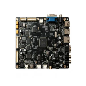
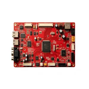
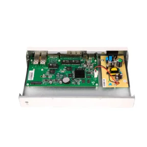
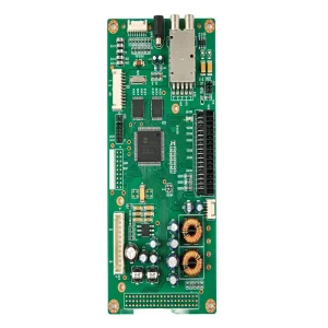
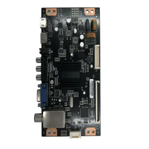
Integrated electronics manufacturing services: from bare board stack-up simulations to fully verified, box-built mission-critical assemblies.
Modern electronic systems no longer tolerate the fragmented handoff between CAD design bureaus and assembly floors. Discover how factory-integrated PCB layout design unlocks unparalleled yield and signal fidelity.
Gigabit interfaces (PCIe 4.0/5.0, DDR4/DDR5, USB4) necessitate nanosecond-accurate length matching, dielectric-controlled impedance profiling, and low-loss return current loop optimization. Our in-house layout engineers simulate transmission lines prior to panelization, mitigating crosstalk, ringings, and reflection at the physical copper level.
Over 74% of manufacturing delays stem from component footprint mismatches, tombstoning risks, and insufficient solder dam clearances. By aligning IPC-7351B standards with live factory SMT tooling data, our OEM layout services design land patterns tailored precisely for automated stencil apertures and thermal reflow dynamics.
Unlike independent layout contractors, our engineering workflow feeds directly into our Bao'an, Shenzhen factory MES (Manufacturing Execution System). Every trace geometry, thermal relief pad, and testpoint array is verified against real pick-and-place coordinate tolerances, ensuring seamless NPI (New Product Introduction) and mass replication.
Engineered for high-density interconnects (HDI), complex mixed-signal circuits, and harsh thermal environments. We validate your layout tolerances against direct production constraints.
| Layout & Routing Densities | Single-sided, double-sided, multilayer rigid boards (up to 48 layers), High-Density Interconnect (HDI 1+N+1 through Any-Layer microvia processes), Rigid-Flex, and Aluminum/Metal Core PCBs. |
|---|---|
| CAD Tooling Compatibility | Altium Designer, Cadence Allegro & OrCAD, Mentor Graphics PADS, Siemens Xpedition, KiCad. Complete delivery includes Native Schematics, PCB Binaries, Gerber RS-274X / ODB++, IPC-2581, and Centroid Pick-and-Place data. |
| High-Speed SI/PI Competencies | Impedance control down to ±5% tolerance (single-ended 50Ω, differential 90Ω/100Ω), serpentine delay tuning, crosstalk isolation guard traces, plane splitting, and power distribution network (PDN) loop inductance mitigation. |
| Minimum Trace Width / Spacing | Inner layers: 2.5 mil / 2.5 mil (0.063mm); Outer layers: 3.0 mil / 3.0 mil (0.075mm). Laser direct imaging (LDI) applied for extreme edge definition and fine-pitch BGA breakouts (down to 0.35mm pitch). |
| Drill & Aspect Ratio Limits | Mechanical drill min: 0.15mm (6 mil); Laser microvia min: 0.075mm (3 mil); Blind, buried, stacked, and staggered microvias. Maximum board aspect ratio up to 12.5:1. Via-in-Pad Plated Over (VIPPO) standard. |
| Surface Finishes & Substrates | Standard FR-4 (Tg 140°C to 180°C+), Rogers high frequency, Megtron 6, Shengyi, Nelco, Polyimide flex cores. Surface finishes: ENIG, ENEPIG, Immersion Silver, Immersion Tin, Hard Gold, and Lead-Free HASL. |
| Production Line Footprint | Shenzhen Bao'an facility: 7 automated high-speed SMT lines (Yamaha/Panasonic pick-and-place), 2 DIP/THT lines with selective wave soldering, 2 dedicated functional test lines, and 2 box-build assembly cells. |
| Acceptance Criteria | Class 2 and Class 3 IPC-A-610 standards, IPC-6012, IPC-2221, ISO 9001, IATF 16949 (Automotive), ISO 13485 (Medical Devices), and ISO 14001 Environmental Management Systems. |
Leveraging the world's most concentrated electronics industrial cluster to compress layout iterations, eliminate component shortages, and expedite mass production.
Situated in the heart of Shenzhen's Bao'an electronics cluster, our procurement division maintains real-time APIs to over 100 franchised tier-1 component distributors and factory-direct silicon lines. With immediate access to 500,000+ authenticated part numbers, we navigate passive shortages, verify date codes, and guarantee batch authenticity.
Layout modifications often cripple overseas lead times when communication loops cross disconnected vendors. At our factory, engineering change orders (ECOs) are transferred to the SMT setup within hours. Prototypes are verified on rapid-response lines, allowing customers to transition from layout signoff to physical PCBA samples in as few as 3 to 5 business days.
During the PCB layout phase, our experienced hardware engineers analyze your bill of materials (BOM) against high-runner domestic and international parts. We identify pin-compatible, drop-in alternative components for passives, connectors, and power regulators that drastically trim overall bill-of-materials costs without sacrificing electrical reliability or agency approvals.
Global supply chain directors and sourcing executives face mounting pressure around intellectual property protection, supply transparency, and zero-defect quality mandates.
Strict NDAs are executed prior to schematic ingestion. All layout databases, gerbers, and firmware files reside on encrypted, air-gapped engineering networks protected by biometric access and comprehensive audit logging.
Our operation is independently accredited under IATF 16949 for automotive zero-defect standards, ISO 13485 for medical life-support reliability, ISO 9001 for quality governance, and ISO 14001 for environmental stewardship.
Whether testing 5 proof-of-concept prototype boards or ramping up to 500,000 units on automated Panasonic SMT lines, our lines offer complete batch agility without punitive minimum order quantity restrictions.
With an audited 99.5% on-time delivery record, we manage express air, ocean consolidation, and DDP shipments to engineering hubs across North America, the European Union, South America, and the Asia-Pacific region.
Passing CE, FCC, UL, and regional safety audits begins on the layout CAD screen. Here is how our physical engineering protects your electronic products from costly field recertifications.
We apply deliberate trace geometries, continuous ground reference planes, split isolation boundaries, and ferrite bead filter placements. This minimizes common-mode radiation and loop antennas, assuring seamless adherence to FCC Part 15 Class B and EN 55032/CISPR 32 standards for radiated emissions.
For power supply designs, buck converters, and high-voltage industrial drivers, layout engineers calculate exact creepage distances along board surfaces and clearance gaps across open air. We integrate CNC isolation routing slots beneath optocouplers and transformers to eliminate dielectric arcing risks.
All fabricated bare boards and procured active/passive components are verified lead-free (Pb-free) in full conformity with RoHS Directive 2011/65/EU and EU 2015/863. Full laboratory test reports and material declaration datasheets are cataloged for your regulatory technical files.
From wide-bandgap GaN/SiC power electronics to on-device edge AI micro-architectures, modern layouts require specialized layout engineering.
AI accelerators, NPUs, and edge computing SoCs generate intense localized thermal flux. Our layouts incorporate thermal via farms, embedded heavy-copper planes (up to 6 oz), and aluminum metal cores to conduct heat efficiently toward heat sink interfaces without causing solder fatigue.
Gallium Nitride (GaN) and Silicon Carbide (SiC) switching devices operate at MHz frequencies with nanosecond rise times. Our layout engineers master parasitic loop inductance minimization to prevent high dV/dt voltage spikes and false gate trigger events.
Wearables and portable medical gadgets demand ultra-fine geometries. We utilize laser microvias, stacked via structures, and thin core polyimide materials to route multi-bus 0.35mm pitch BGAs into compact, lightweight multi-board flex-rigid assemblies.
Explore how our turnkey OEM PCB layout, fabrication, and assembly services provide direct sector-specific solutions worldwide.
Engine control units, BMS battery monitoring modules, in-cabin telematics, and radar sensors. Engineered strictly according to IATF 16949 standards, high-vibration design rules, and thermal shock resilience.
Class II/III medical devices, non-invasive diagnostic monitors, and blood gas analyzers. Built under ISO 13485 cleanroom protocols with lot-level component traceability and conformal coating moisture protection.
PLC controllers, motor drive inverters, load balancers, and industrial IoT gateways. Designed with galvanic optical isolation, surge suppressors, and thick-copper reliability for continuous 24/7 runtimes.
Solar inverter boards, DC-DC buck converters, EV charging interfaces, and intelligent energy metering assemblies. Engineered with maximum thermal copper planes and certified dielectric creepage spacing.
Direct answers to the questions global engineering directors, hardware architects, and sourcing specialists ask most.
To begin a custom layout project, we require: (1) Detailed schematic diagram (in native Altium, OrCAD, Eagle, or searchable PDF format); (2) Bill of Materials (BOM) including exact manufacturer part numbers and preferred footprint designations; (3) Mechanical enclosure step files or 2D DXF board outline drawings with connector locations and keep-out zones; and (4) Critical design rules such as high-speed net lists, differential impedance targets, and power tree ratings.
Our layout engineering team utilizes industry-standard simulation software to analyze transmission lines, calculate dielectric heights, and simulate return path loops. For differential pairs (e.g., PCIe, USB 3.0, Ethernet, LVDS), we enforce strict length matching down to ±5 mils and isolate high-speed signals between continuous solid ground reference planes to prevent EMI crosstalk and signal degradation.
Yes. If you have an legacy hardware product without native CAD databases, our engineering lab can perform high-precision multilayer delamination, X-ray scanning, and schematic netlist extraction. We reconstruct updated, modernized schematic schematics and Altium/Gerber layout files while substituting obsolete or end-of-life (EOL) components with readily available equivalents.
Standard turnaround for layout design depends on pin count and density: simple 2-4 layer layouts require 3–5 working days, while complex 8–16 layer HDI layouts require 10–15 working days. Once the layout and DFM signoff are completed, quick-turn bare PCB fabrication and SMT prototype assembly can be delivered in as rapidly as 3 to 7 working days, enabling fast validation cycles.
Confidentiality is fundamental to our OEM partnerships. We sign bilateral Non-Disclosure Agreements (NDAs) prior to receiving any design materials. Design files are segregated on encrypted departmental file servers accessible only by dedicated project engineers. No project assets are shared with third parties or outside suppliers without prior written authorization.
Our Shenzhen factory operates two dedicated test lines equipped for: (1) Automated Optical Inspection (AOI) checking 100% of solder joints; (2) High-resolution 3D X-ray inspection for BGA and QFN voiding analysis; (3) In-Circuit Testing (ICT) and Flying Probe testing for circuit continuity; and (4) Customized Functional Testing (FCT) powered by customer-provided firmware or diagnostic test fixtures.
Browse our diverse portfolio of custom OEM electronic assemblies, serving global clients across industrial, environmental, and consumer sectors.