Explore production-grade electronic assemblies manufactured for high-reliability medical, enterprise networking, industrial robotics, and intelligent IoT environments.
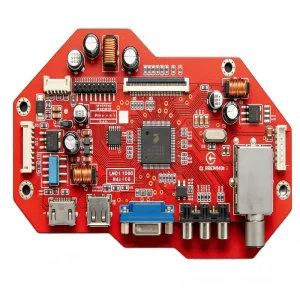
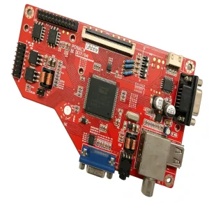
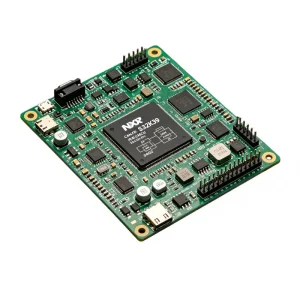

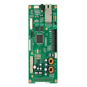
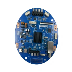
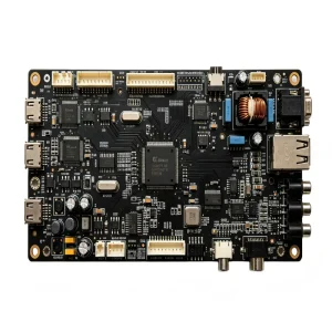
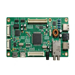
In the contemporary hardware manufacturing environment, global technology OEMs face a paradigm shift characterized by shrinking product lifecycles, exponential silicon miniaturization, and intricate multi-tier supply chain dynamics. Procuring electronic manufacturing services (EMS) is no longer a simple transactional bidding exercise; it has matured into a multi-dimensional strategic partnership focused on Total Cost of Ownership (TCO) optimization, supply resiliency, and verifiable quality engineering.
High-reliability sectors—including aerospace displays, implantable and non-invasive medical hardware, automotive control units, and renewable grid inverters—demand zero-defect tolerances. Selecting an accredited turnkey PCBA manufacturer in Shenzhen requires scrutinizing whether a supplier merely populates circuits or proactively eliminates manufacturability bottlenecks through rigorous upfront Design for Manufacturing (DFM), Design for Assembly (DFA), and Design for Testability (DFT) protocols.
Furthermore, post-pandemic geopolitical volatility has heightened the value of integrated, single-point accountability. When bare board fabrication, component procurement, surface-mount placement, through-hole soldering, firmware flashing, conformal coating, and final box-build testing are executed within a unified ERP/MES environment, enterprises prevent costly finger-pointing between disjointed suppliers, compress time-to-market by up to 40%, and safeguard their core intellectual property.
Global component shortages require strategic direct distributor alliances with Arrow, Avnet, Digi-Key, Mouser, and verified Tier-1 franchise networks, delivering authenticated components with traceable lot codes and zero counterfeit risk.
Supporting down to 01005 passives, 0.35mm pitch ultra-fine BGAs, PoP (Package-on-Package), and micro-via high-density interconnect (HDI) structures with automated multi-zone nitrogen reflow optimization.
Seamless progression from bare substrate fabrication to cable-harness assembly, bespoke aluminum enclosure integration, ultrasonic welding, environmental potting, and customized retail or protective packaging.
Our Shenzhen production hub is equipped with high-speed Yamaha and Fuji SMT lines, Heller reflow ovens, and Koh Young 3D SPI/AOI optical metrology, operating within the tightest engineering parameters.
| Manufacturing Parameter | Standard Production Capabilities | Advanced / High-Density Limits | Quality Standards & Assurance |
|---|---|---|---|
| Layer Count & Stack-up | 1 – 28 Layers (Rigid FR-4) | Up to 64 Layers (Rigid-Flex, HDI Any-Layer) | IPC-6012 Class 3 |
| Min. Trace Width / Spacing | 3.5 mil / 3.5 mil (0.089mm) | 2.0 mil / 2.0 mil (0.050mm) fine line | Laser Direct Imaging (LDI) |
| Surface Mount Pitch | 0.4mm BGA / QFN pitch | 0.30mm BGA pitch, 01005 passive placement | 3D AOI & 3D AXI Verified |
| Substrate Materials | Standard FR-4 (Tg 140°C - 170°C) | Rogers, Megtron 6, Polyimide Flex, Ceramic, Aluminum | RoHS / REACH Compliant |
| Via Technologies | Through-hole, blind & buried vias | Stacked micro-vias, via-in-pad copper plated | IPC-4761 Type VII Capped |
| Surface Finishes | HASL lead-free, ENIG (Electroless Nickel) | ENEPIG, Hard Gold (30u"), Immersion Tin/Silver | MIL-STD-883 Gold Wire Bondable |
| Soldering Atmospheric Environment | Air convection multi-zone reflow | Nitrogen (N2) atmosphere, vacuum vapor phase | Voiding rate < 5% on thermal pads |
Two decades of rigorous process control reflected in verifiable performance indicators.
Every engineering step is governed by barcode traceability in our MES platform, ensuring end-to-end quality transparency from bill-of-materials ingestion to final consignment delivery.
Comprehensive review of Gerber RS-274X/ODB++, BOM part numbers, footprint solderability, annular ring integrity, and copper clearances prior to copper strike.
Automated API integration with verified global distributors, conducting incoming electrical verification, date-code checks, and vacuum-sealed moisture dry-pack storage.
High-precision laser direct imaging, multi-layer hot pressing, automated optical inspection of inner layers, controlled impedance coupons, and flying-probe electrical tests.
Laser cut stencils, 3D Solder Paste Inspection (SPI), high-speed dual-beam chip mounters, and 10-zone reflow profiles calibrated to specific component thermal masses.
Automated lead-free dual-wave soldering or programmable selective soldering machines for sensitive through-hole connectors, electrolytic caps, and power inductors.
100% automated optical inspection of solder joint fillets, followed by high-resolution 3D X-ray tomography to detect microscopic voids beneath BGA and QFN packages.
Microcontroller IC programming, custom test-bed functional circuit testing (FCT), In-Circuit Testing (ICT), and thermal burn-in under dynamic electrical loads.
Robotic silicone/acrylic conformal coating for harsh environments, wire-harness routing, mechanical enclosure integration, and antistatic ESD vacuum packing.
Engineered to conquer the hostile operating conditions of industrial vibrations, automotive temperature excursions, and sterile healthcare environments.
IATF 16949 compliant assemblies for EV DC-DC converters, Battery Management Systems (BMS), On-Board Chargers (OBC), and ADAS sensing controllers with AEC-Q200 components.
ISO 13485 certified PCBA manufacturing for critical patient monitors, surgical imaging displays, portable ultrasound devices, and telemetry implants with lot-level traceability.
Heavy copper (up to 10oz) PCBs, high-voltage solar microinverters, industrial programmable logic controllers (PLCs), motor drives, and outdoor environmental restoration sensors.
Low-loss high-speed substrates (Rogers 4350B, Panasonic Megtron), controlled impedance testing (TDR ±5%), mmWave transceivers, and enterprise 10GbE network switching fabrics.
As standard monolithic silicon architecture approaches traditional thermal and lithographic limitations, the electronics manufacturing ecosystem is moving toward heterogeneous integration. System-in-Package (SiP), embedded active components within substrate inner cores, and high-density rigid-flex integrations are transforming conventional PCBA from mechanical mounting substrates into active silicon interposers.
In response to these demands, modern smart factory floors are incorporating AI-driven predictive metrology. Convolutional neural networks (CNNs) integrated into automated 3D optical and X-ray systems continuously cross-reference real-time solder meniscus volume, wetting angles, and solder-paste height with downstream thermal profile anomalies. This transition from reactive defect inspection to closed-loop predictive process stabilization reduces scrap rates to near-zero PPM levels.
Environmental governance is also evolving beyond baseline European RoHS and REACH mandates. Tier-1 OEMs increasingly prioritize lifecycle carbon audits, bio-based flame-retardant laminate formulations, low-temperature soldering (LTS) alloys that curtail oven energy consumption by 25%, and closed-loop water treatment facilities that recycle 98% of hazardous electroplating rinses.
Transitioning from discrete QFN/BGA packaging toward 2.5D substrate interposers, embedded passives, and sub-30μm copper pillar interconnects for hyper-dense edge-computing hardware.
Real-time machine-to-machine (M2M) feedback between 3D SPI and solder paste printers, dynamically adjusting squeegee pressure, speed, and stencil separation on a per-board basis.
Adoption of lead-free, antimony-free, and halogen-free high-Tg resins paired with bismuth-doped SAC alloys to decrease thermal stress during multi-cycle reflow sequences.
Third-party accredited quality management systems guarantee compliance with stringent automotive, medical, industrial, and environmental directives.
Automotive grade quality management ensuring robust APQP, FMEA, PPAP submission, and zero-defect production methodology.
Medical device quality assurance covering rigid traceability, environmental cleanrooms, and risk management through EN ISO 14971.
Foundational quality management structure governing global procurement, design engineering reviews, and customer satisfaction metrics.
Environmental stewardship verifying responsible chemical disposal, RoHS & REACH compliance, and energy-efficient factory operations.
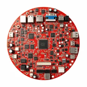
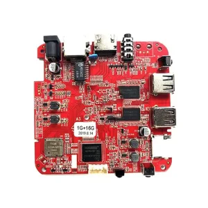
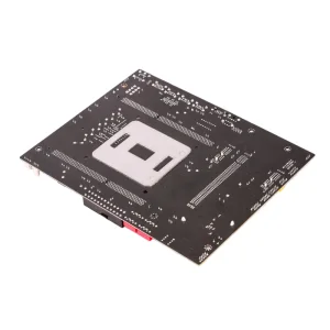
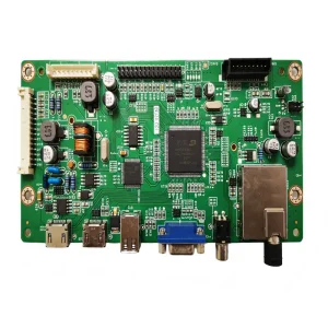
Production assemblies built for demanding power conversion, green energy grids, portable medical ultrasound, and smart automation.
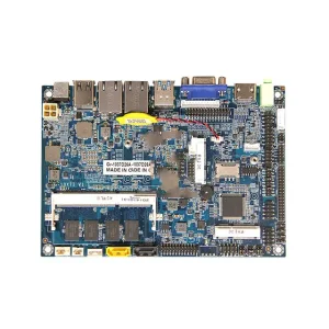
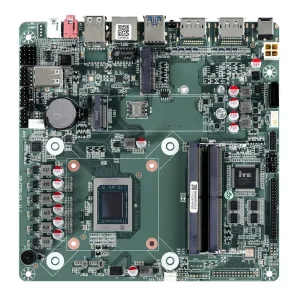

Comprehensive engineering and commercial answers addressing intellectual property protection, minimum order economics, component lead times, and quality standards.
We maintain direct API-connected procurement ties with authorised global franchised distributors, including Digi-Key, Mouser, Arrow, Avnet, and original component manufacturers (OCMs). Every incoming shipment undergoes mandatory visual package verification, barcode batch verification, pin-solderability inspection, and X-ray die analysis for high-risk active integrated circuits.
Quick-turn prototype assemblies can be completed in as little as 24 to 48 hours following component arrival and DFM sign-off. High-volume series production runs generally require 15 to 20 working days, depending on bare PCB complexity (e.g., heavy copper or HDI blind/buried micro-vias) and specialized component lead times.
Before reviewing Gerber files, BOMs, or firmware, we execute bilateral Non-Disclosure Agreements (NDAs). Design files reside on air-gapped, encrypted internal servers accessible solely to assigned project engineers. Physical firmware programming cells operate with locked code flashing fixtures, preventing unauthorized firmware extraction.
To generate an accurate engineering quote within 24 hours, we require: (1) Gerber data in RS-274X or ODB++ format including layer stackup; (2) Detailed Bill of Materials (BOM) detailing manufacturer part numbers (MPN), approved alternate parts, and reference designators; (3) Centroid / Pick-and-Place file; (4) Testing instructions / specifications.
Yes. We operate flexible, fast-changeover SMT lines tailored for high-mix, low-to-medium volume builds alongside dedicated mass-production lines. This lets startups and enterprise R&D teams validate engineering prototypes and pilot batches under the exact same IATF 16949 / ISO 13485 quality conditions as volume production runs.
Each PCB panel is laser-etched with a high-density 2D data-matrix barcode at bare board inception. Our Manufacturing Execution System (MES) links this code to solder paste lots, SMT feeder stations, reflow oven temperature profiles, technician IDs, and functional circuit test data, providing complete unit-level provenance for safety-critical audits.
Connect directly with our Shenzhen engineering headquarters. Submit your Gerber files and BOM today for a complete DFM manufacturability evaluation, component cost breakdown, and rapid turnaround schedule.
