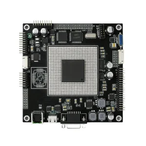
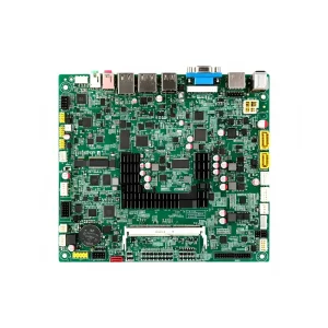
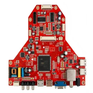
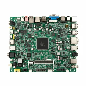
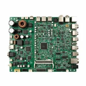
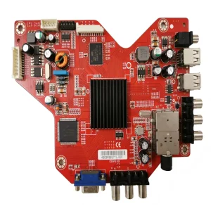
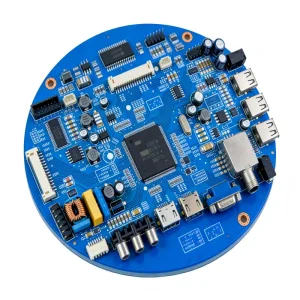
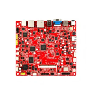
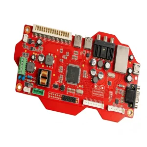
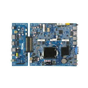
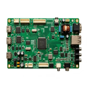
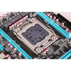
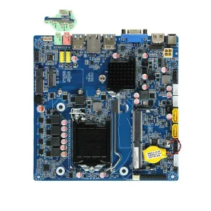
Exemplifying our certified assembly capabilities across industrial control systems, automotive modules, optoelectronics, and power conversion electronics.
In an era marked by geopolitical volatility, accelerated product life cycles, and escalating miniaturization demands, choosing an Original Equipment Manufacturer (OEM) PCB partner requires deep technical alignment, rigorous risk management, and scalable infrastructure.
Global tier-1 OEMs no longer evaluate contract manufacturers based purely on unit PCB cost. Comprehensive TCO analysis encompasses Design for Manufacturability (DFM) yield impacts, component obsolescence hedges, duty structures, and localized field-failure mitigation.
The global proliferation of grey-market silicon demands absolute supply chain transparency. A certified OEM partner leverages direct factory distribution agreements and in-house component authentication laboratories to safeguard critical production runs.
Bridging the gap between initial hardware validation and sustained high-volume fabrication demands parallel engineering. Quick-turn engineering lines prevent prototype delays while production automated lines stand ready for high-throughput scaling.
Shenzhen remains the undisputed global capital of electronics hardware innovation. Our centralized facility in Bao'an District unlocks unparalleled supply chain density, radical turn-around velocity, and engineering depth.
Within a 30-kilometer radius, over 500,000 passive, discrete, and active component variants are directly accessible from manufacturer warehouses and tier-1 franchised distributors.
PCB fabrication never operates in isolation. Shenzhen offers tight synergy between bare circuit boards, custom metal stamping, plastic injection enclosures, and silicone membrane switch development.
With a dedicated team of over 50 seasoned hardware, layout, and manufacturing engineers, our clients gain access to deep process knowledge spanning IPC Class 2 and Class 3 reliability criteria.
Strategically adjacent to Hong Kong International Airport (HKG) and Shenzhen Bao'an (SZX), finished assemblies clear bonded export hubs within hours, ensuring strict delivery timelines worldwide.
From prototype validation to mass automated deployment, review our precise manufacturing tolerances and process limits validated under IATF 16949 and ISO 13485 quality systems.
| Manufacturing Dimension | Standard Capability | Advanced / High-Density Interconnect (HDI) |
|---|---|---|
| Layer Count & Substrates | 1 – 28 Layers (Standard FR-4, Aluminum, Copper Core) | Up to 48 Layers (Rogers, Megtron 6, Polyimide Flex, Rigid-Flex, Ceramic) |
| SMT Placement Velocity & Accuracy | 0201 passives, SOIC, QFP, standard pitch ICs | 01005 passives, ultra-fine 0.3mm pitch BGA, Micro-CSP, PoP (Package-on-Package) |
| Minimum Line Width / Spacing | 3.5 mil / 3.5 mil (0.089 mm) | 2.0 mil / 2.0 mil (0.05 mm) with laser direct imaging (LDI) |
| Through-Hole & Micro-Via Tech | Mechanical drilling: Min 0.15mm hole diameter | Laser drilled blind & buried micro-vias, staggered/stacked, copper filled |
| Surface Finishes | HASL, Lead-free HASL, OSP, Immersion Tin | ENIG (Electroless Nickel Immersion Gold), ENEPIG, Immersion Silver, Hard Gold Plating |
| Inspection & Verification Suite | Multi-angle 2D AOI, First-Article Inspection (FAI) | High-resolution 3D Inline AOI, 3D Real-time X-Ray (AXI), Flying Probe, In-Circuit Test (ICT) |
| Post-Assembly Value-Add | Manual soldering, simple functional jigs | Robotic Conformal Coating (Acrylic, Polyurethane, Silicone), Ultrasonic Welding, Box Build |
Modern PCB manufacturing is fundamentally transforming under the dual pressures of AI-driven edge hardware and high-voltage electrified mobility. We stay ahead of industry demands.
With the integration of neural processing units (NPUs) into localized edge computers, thermal dissipation becomes paramount. Modern PCBA designs demand heavy-copper layers (up to 6oz), integrated vapor chambers, and embedded coin technology to dissipate extreme heat densities without thermal throttling.
The explosion of 5G infrastructure, satellite IoT, and gigahertz-level automotive radar demands precise signal integrity. Controlling dielectric constants (Dk) and dissipation factors (Df) requires hybrid stackups, integrating low-loss hydrocarbon ceramics with standard FR-4 prepregs.
Global legislation including EU RoHS 3, REACH, and WEEE directives are establishing strict guidelines for eco-friendly electronics. Sustainable manufacturing requires energy-efficient nitrogen reflow profiles, water-soluble flux chemistries, and certified lead-free solder metallurgy.
Every industry presents unique operating environments. Whether operating in sub-zero aerospace altitudes or inside sterile medical telemetry systems, our production workflows conform to certified industry standards.
Built strictly under IATF 16949 protocols. Applications include advanced driver-assistance systems (ADAS), battery management systems (BMS) for electric vehicles, and onboard telematics units subjected to rigorous thermal shock cycles.
Executing precision assembly under ISO 13485 quality management. Products range from portable diagnostic pulse oximeters to hospital-grade monitor power modules demanding low leakage current and high isolation barrier integrity.
Heavy machinery, programmable logic controllers (PLCs), and variable frequency motor drives require robust surge protection, heavy copper trace thicknesses, and vibration-resistant solder joint reliability according to IPC-A-610 Class 3 standards.
Ultra-compact, low-power connected ecosystems such as mesh gateways, smart garage controls, and acoustic noise monitors. Leveraging ultra-miniature package footprints and fine-pitch radio frequency modules for reliable consumer deployments.
Clear, definitive technical answers addressing intellectual property protection, supply chain lead times, quality gating, and overseas logistics.
We enforce strict IP security protocols starting with mutually binding, legally robust Non-Disclosure Agreements (NDAs) prior to receiving Gerber or BOM files. In production, our enterprise ERP and MES run on isolated, air-gapped internal servers with encrypted storage. Firmware flashing occurs via authenticated automated tools without direct engineering operator access to binary source code, ensuring zero file exfiltration.
Quick-turn prototype PCB fabrication and assembly can be expedited in as fast as 24 to 72 hours once components are on hand. Standard turnkey prototype lead times typically run 7 to 10 working days, incorporating comprehensive DFM/DFA engineering reviews. Volume production runs typically require 3 to 4 weeks depending on raw material lead times and component market availability, which we buffer through tailored vendor-managed inventory programs.
Yes. Our dedicated BOM engineering team cross-references your parts list across global component databases to flag End-of-Life (EOL), Not Recommended for New Designs (NRND), and volatile single-source ICs. We propose drop-in pin-to-pin functional equivalents or secondary footprint recommendations that can reduce procurement costs by 15% to 35% without requiring PCB schematic changes.
Quality assurance operates on a multi-stage verification matrix. Solder paste application is inspected via 3D SPI; post-reflow inspection utilizes high-speed 3D AOI for misalignments, bridging, and solder volume. Complex ball grid arrays (BGA) and QFNs undergo 3D Automated X-ray Inspection (AXI) for void ratio verification. Finally, custom functional test fixtures (FCT), flashing stations, and high-voltage burn-in chambers validate end-device operational performance.
We support versatile commercial shipping models including Delivered Duty Paid (DDP), Free On Board (FOB), and EXW terms. Leveraging direct customs integration at Shenzhen and Hong Kong shipping hubs, we handle all Harmonized System (HS) code classifications, export documentation, certificate of origin filings, and commercial invoicing. We work with leading carriers (DHL, FedEx, UPS, freight forwarders) to ensure smooth international delivery.
Demonstrating our production versatility across high-speed computing, medical telemetry, smart displays, environmental sensors, and consumer communications.