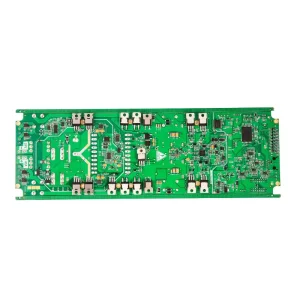
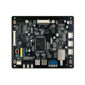
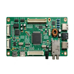
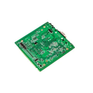
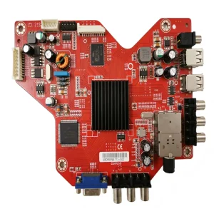
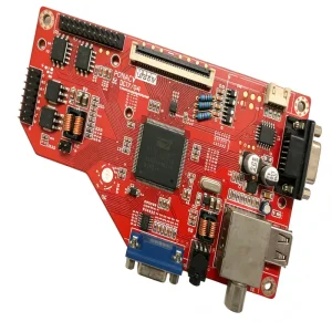
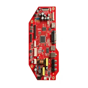
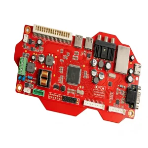
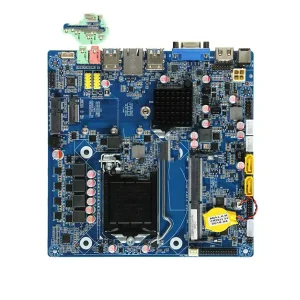
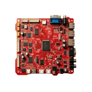
Explore integrated manufacturing executions across automotive power conversion, smart aviation, and advanced IoT telemetry assemblies engineered at STHL factory facilities.
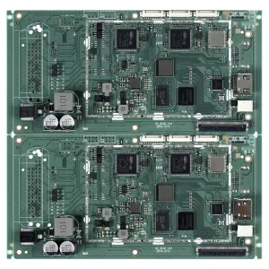
The global printed circuit board assembly (PCBA) and original equipment manufacturer (OEM) electronics manufacturing services (EMS) sector has entered an inflection point driven by miniaturization, the electrifying automotive transition, Edge AI deployment, and mission-critical medical sensorization. Modern industrial procurement has evolved from transactional component assembly toward high-level end-to-end integration. Global enterprises no longer view PCB fabrication and assembly as decoupled stages; fragmented multi-vendor handling introduces unquantifiable risks in thermal mechanical tolerance, cross-vendor supply chain friction, intellectual property leakages, and impedance mismatches.
Established in 2006 in Bao'an, Shenzhen—the epicenter of global electronics innovation—Shenzhen STHL Electronics Co., Ltd. (STHL) operates a specialized 10,000+ m² smart manufacturing plant equipped with 7 high-speed SMT lines, 2 automated DIP/THT lines, 2 dedicated functional test suites, and 2 box-build assembly corridors. As industrial equipment and consumer ecosystems demand higher signal integrity, denser layout pitch (down to 0.3mm BGA pitch and 01005 passives), and zero-defect longevity, OEM manufacturing partners must establish seamless traceability bridging raw substrate lamination to final cloud firmware flashing.
STHL deploys enterprise-grade Manufacturing Execution Systems (MES) synchronized with cloud ERP platforms. Every surface-mount component reel, bare laminate batch, and solder paste jar is tracked via serialized 2D datamatrix codes, enabling sub-millimeter lifecycle auditability compliant with IATF 16949 (Automotive), ISO 13485 (Medical Devices), ISO 9001 (Quality), and ISO 14001 (Environmental) regulatory mandates.
From automated optical inspection augmented by deep learning to lead-free metallurgical controls, our facilities incorporate five core technological shifts.
Traditional 2D threshold-based optical inspection is superseded by deep-learning machine vision. Our 3D Solder Paste Inspection (SPI) and Automated X-ray Inspection (AXI) accurately measure voiding ratios, solder fillet heights, and micro-bridging beneath Quad Flat No-leads (QFN) and Ball Grid Arrays (BGA) without false-positive line stoppages.
Shrinking silicon die configurations necessitate sequential laminar builds. STHL factory suites routinely manufacture any-layer microvia substrates, stacked microvias (1+N+1 to 4+N+4), and copper-filled via-in-pad structures, ensuring high signal speeds and low loop inductances for dense computing hardware.
RoHS and REACH compliance demand stringent reflow thermal window profiling. Utilizing 10-zone nitrogen-purged convection ovens and real-time thermocouple data loggers, reflow peaks are precisely calibrated between 235°C and 245°C to avoid delta-T thermal shock across diverse thermal masses.
In accordance with IATF 16949 automotive standards, critical circuits such as On-Board Chargers (OBC) and Body Control Modules (BCM) undergo lot-specific tracking. Solder paste stencil volume, pick-and-place nozzle speed, and conformal coating thickness are documented against individual serial IDs.
Space-constrained medical implants and aerospace avionics displays demand combined polyimide flex circuits with rigid FR-4 backings. Our specialized laser-routing and differential depth controlled milling ensure mechanical durability across millions of bend cycles.
Moving past bare PCBA boards, modern OEMs require full turnkey enclosure integration. STHL accommodates precision ultrasonic welding, potting encapsulation, robot-assisted screw driving, custom cable harness pinning, and end-of-line wireless RF link validation.
Different operating environments dictate divergent manufacturing priorities, test parameters, and protective coatings.
| Industry Sector | Typical OEM Assemblies | Critical PCB Engineering Challenges | STHL Quality Validation Protocol |
|---|---|---|---|
| Automotive & EV Power | On-Board Chargers (OBC), Inverters, Body Control Modules (BCM) | High current dissipation, thermal stress cracking, vibration damping, copper weights >3oz. | IATF 16949 PPAP Level 3, Thermal Shock (-40°C to +125°C), Automated Potting, Hi-Pot Electrical Isolation. |
| Medical & Healthcare | Pacemakers, Clinical Thermometers, Multiparameter Monitors | Zero contamination, biocompatible soldering, high impedance isolation, sub-millimeter component density. | ISO 13485 Cleanroom Assembly, Ionic Contamination Testing (IPC-TM-650), 100% Micro-focus 3D X-Ray Inspection. |
| Aerospace & Avionics | Primary Flight Displays (PFD), Navigation Telemetry, Power Regulation | Extreme altitude decompression, vibrational harmonic resonance, zero tin-whisker tolerances. | Conformal coating (Silicone/Polyurethane to IPC-CC-830), Flying Probe Testing, ENIG/HASL Lead-tolerant processing. |
| Smart Home & IoT | Smart Thermostats, Gas Leak Detectors, Intercom Hubs, Voice Nodes | RF signal attenuation, battery-optimized parasitic draw, miniature form-factors, high volume cost target. | Vector Network Analyzer (VNA) RF antenna calibration, automated ICT (In-Circuit Testing), low-power sleep current testing. |
| Industrial Power & Controls | Motor Drives, Smart Energy Metering, Solar Inverters, Safety Alarms | Transient voltage suppression, extended operating duty life (>10 years), harsh atmospheric corrosion. | Thick copper processing, Selective Automated Soldering, Automated Conformal Dip Coating, Burn-in Environmental Chambers. |
From Gerbers and BOM ingestion to outbound shipment, our production gates guarantee zero defect slippage.
Comprehensive design-for-manufacturability and design-for-assembly checks on pad spacing, aspect ratios, annular rings, and solder dam geometries.
Traceable component purchasing via authorized distributors (Arrow, Avnet, Digi-Key, Mouser) mitigating gray-market counterfeit risks.
High-speed surface mounting down to 01005 passives and 0.3mm BGA pitch, followed by selective through-hole soldering in nitrogen envelopes.
Multistage verification including 3D SPI, automated optical inspection, 3D X-ray inspection, boundary scan, and full functional firmware test benches.
How STHL resolves the tri-fold pressures of silicon obsolescence, cross-border tariff complexity, and dynamic prototyping cycles.
Component lifecycles have compressed dramatically. STHL's engineering team provides active BOM scrub reviews, pin-to-pin drop-in replacement suggestions, and redesign-for-cost (DFC) optimizations that mitigate redesign cycle stalls when semiconductors reach End-of-Life (EOL).
Exporting to over 90 countries—including North America, Germany, the UK, Poland, and Brazil—our logistical framework adheres to international trade export standards, custom-cleared DDP arrangements, RoHS/REACH declarations, and UL94V-0 flammability certifications.
Hardware startups and enterprise R&D groups often face friction moving from pilot run to mass production. We impose zero Minimum Order Quantities (No MOQ), operating prototype lines on identical high-yield equipment as volume runs to ensure frictionless ramp-up.
Specialized controller boards, medical sensor modules, biometric instruments, and home automation hardware produced under certified cleanroom parameters.
Clear, technical explanations covering capability thresholds, intellectual property protections, and supplier evaluation criteria.