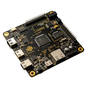
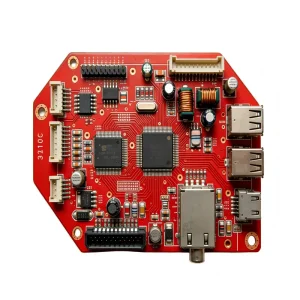
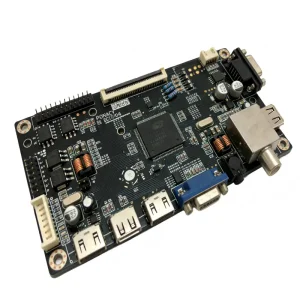
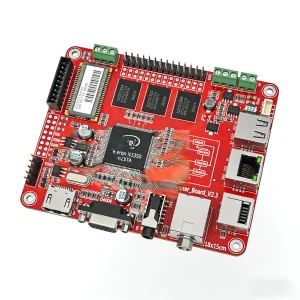
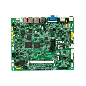
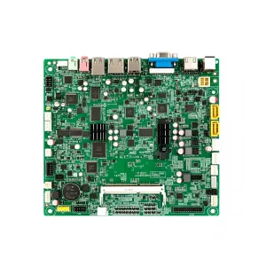
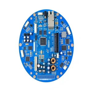
Our turnkey surface-mount (SMT) and through-hole (THT) lines manufacture high-yield assemblies engineered for tight-tolerance, hazardous-environment, and safety-critical duty cycles.

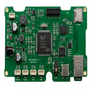
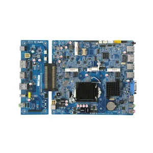
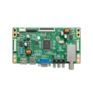


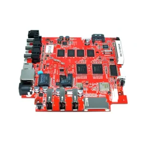
Analyzing modern electronics manufacturing imperatives: Micro-pitch architectures, thermal management, regulatory oversight, and zero-defect yield enforcement across tier-one applications.
The contemporary electronics market continues to endure severe supply chain perturbations, giving rise to remarketed, re-tooled, and cloned active silicon. A robust OEM PCBA partner must institute rigorous incoming raw-material inspection policies, encompassing optical microscopies, decapsulation acid-etch sampling, and X-ray fluorescence (XRF) elemental material characterization to prevent catastrophic systemic field failures.
As microelectronics shift towards 01005 passive package components, ultra-fine-pitch Ball Grid Arrays (BGAs), and Quad-Flat No-Leads (QFNs), standard visual verification is obsolete. Quality control matrices now necessitate integrated in-line 3D Solder Paste Inspection (SPI) correlated via closed-loop feedback to automated screen printers, combined with high-resolution oblique 3D Automated Optical Inspection (AOI).
Global original equipment manufacturers require strict batch-level and individual circuit board accountability. Advanced factories integrate dynamic Manufacturing Execution Systems (MES) alongside real-time Enterprise Resource Planning (ERP), binding unique 2D Data Matrix laser barcoding on raw FR-4 substrates with specific reel lot codes, solder paste expiration lots, and specific reflow oven profile temperature logs.
A breakdown of process quality gates deployed within our manufacturing facilities to eliminate solder abnormalities, mechanical misalignments, component non-conformities, and latent operational drift.
| Manufacturing Stage | Inspection Technology | Target Anomalies Detected | Global Industry Standard |
|---|---|---|---|
| Pre-Production Review | DFM (Design for Manufacturing) & DFA (Design for Assembly) Analysis | Trace clearance violations, insufficient solder pad geometries, thermal relief imbalance, component shadowing | IPC-2221 / IPC-7351B |
| Incoming Raw Materials (IQC) | XRF Spectrometry, Solderability Testing, Moisture Chamber Analysis | Counterfeit internal die, terminal lead oxidation, moisture absorption (MSL Level 3+ risks), lead-free RoHS verification | MIL-STD-202 / J-STD-033 |
| Solder Paste Deposition | High-Speed In-line 3D SPI (Laser Triangulation Profiling) | Paste volume insufficiency, height offsets, bridging, coplanarity deviation, stencil aperture clogging | IPC-A-610 Class 2/3 |
| Post-Reflow SMT Inspection | Dual-Track Multi-Angle 3D AOI & Automated Industrial X-ray (AXI) | BGA hidden solder voiding (>15%), head-in-pillow (HiP) defects, tombstones, component skew, cold solder joints | IPC-A-610 Class 3 / IPC-7095 |
| Post-THT / Wave Soldering | Selective Solder Profile Tracking & High-Res Bottom-Side AOI | Hole-fill insufficiency (<75% barrel fill), excessive solder balls, flux residue contamination, short circuits | IPC-J-STD-001G |
| Subsystem Validation | In-Circuit Testing (ICT), Flying Probe, & Closed-Loop FCT Rig | Parametric drift, wrong component value/polarity, trace open/shorts, firmware flashing mismatch, functional boundary failure | OEM Functional Specifications |
How localized component supply ecosystems, high-density equipment supply chains, and seasoned technical engineers establish unmatched cost advantages and rapid market turnaround times.
Situated within Shenzhen’s high-tech Bao'an ecosystem, our facility procures qualified passives, multilayer substrates, precision tooling, and custom heatsinks within hours rather than weeks. Direct connections to primary component authorized distribution hubs eliminate long intercontinental transits for critical pre-production engineering validation.
With an on-site engineering roster of over 50 technical specialists across layout review, stencil micro-etching, automated test jig programming, and firmware validation, projects transition seamlessly from rapid NPI (New Product Introduction) trial lots of 5 units to massive recurring runs exceeding 100,000 units with zero configuration downtime.
Our operational capabilities extend well beyond basic SMD component population. We accommodate comprehensive mechatronic integration, automated conformal coating lines (acrylic, polyurethane, silicone), ultrasonic wire bonding, potting, and rapid thermal cycling/burn-in chambers to ensure resilient deployment in hostile external conditions.
Our assemblies are deployed globally in highly regulated domains where downtime or system failure carries massive financial or human liabilities.
Electric vehicle (EV) charging hardware, on-board chargers (OBC), and dynamic battery management systems (BMS) require IATF 16949-audited line control, PPAP Level 3 documentation, thermal cycle endurance (-40°C to +125°C), and micro-voiding tolerances below 10% under power QFN thermal pads.
Medical electronics require adherence to ISO 13485 quality protocols, complete lot serialization of sub-components, biocompatible ultrasonic cleaning, and rigorous Class II & Class III electronic traceability with extensive documentation packages ready for FDA / CE MDR submittals.
Process telemetry, gas detectors, buck-boost converters, and safety-critical distributed controls operating within electrically noisy environments. Demands high dielectric breakdown isolation, surge suppression verification, precise conformal coating coverage, and functional thermal soak tests.
In-depth technical answers addressing quality gates, engineering deliverables, testing equipment coverage, and contract manufacturing warranties.
Explore additional high-density PCBA series engineered under our quality management framework for consumer, biometric, communication, and power conversion electronics.