Validated high-density interconnect prototypes ready for scaling from small-batch engineering verification tests (EVT) to mission-critical OEM production runs.
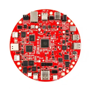
High-speed multi-layer differential pair matching up to 100GbE switching capabilities.
OEM Ethernet Switch PCB Assembly Manufacturer, Factories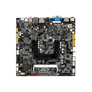
Controlled impedance stack-up optimized for high-bandwidth enterprise gateway hardware.
High-Quality Firewall PCB Assembly Manufacturers, Factory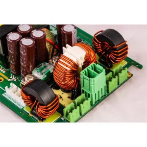
Ultra-compact HDI board prototypes incorporating microvia technology and flexible circuits.
China Tablet PCB Assembly--STHL Manufacturer, Factory
Heavy-copper thermal substrate assembly engineering certified for EV charging stress standards.
China New Energy Vehicle On-board Charging Equipment PCB Assembly Manufacturer, Manufacturers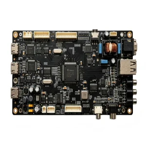
Low-loss dielectric substrates for Wi-Fi 6E/7 and advanced MIMO antenna integration.
OEM Wireless Network Routers PCBA Assembly--STHL Manufacturers, Factory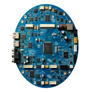
Fine-pitch SMT assembly integrating digital signal processors and Class-D amplifiers.
OEM Smart Speakers PCBA Assembly--STHL Factories, Factory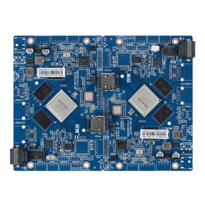
Cost-optimized turnkey board prototyping designed for rapid time-to-market execution.
China Consumer Electronics PCBA Application: Powering the Devices of Tomorrow Manufacturer, Service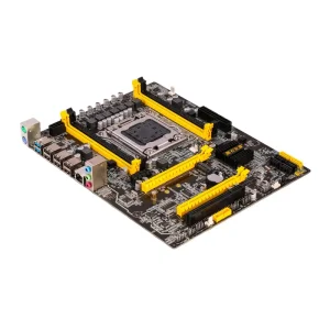
Multi-channel video processing modules supporting 24/7 continuous read/write cycles.
High-Quality NVR PCB Assembly--STHL: Engineering Stable Storage for High-Definition Video-1 Manufacturer, ServiceIn an era marked by rapid hardware iteration cycles, edge computing proliferation, and complex component supply ecosystems, prototype PCB fabrication has transformed from simple board-spinning into a mission-critical risk mitigation stage.
The demand for thinner form factors and edge AI computation necessitates 0.4mm pitch BGAs, 01005 passives, and multi-stage Any-Layer HDI. Prototype boards must reflect true mass-production tolerances at the earliest engineering verification stages.
Global component shortages require pre-assembly engineering analysis. Sourcing teams use prototype stages to validate second-source components, pin-compatible alternative silicon, and lifecycle sustainability before committing capital to tooling.
The separation between prototype assembly houses and volume manufacturing plants is collapsing. Global OEMs now require prototype PCB factories equipped with high-speed automated SMT lines to ensure zero yield degradation during transition.
Standard, advanced, and prototype capabilities audited for mission-critical industrial, medical, and aerospace implementations.
| Capability Parameter | Standard Prototype Capability | Advanced / High-Density Capability | Process Validation Standards |
|---|---|---|---|
| Layer Count & Stack-up | 1 – 16 Layers (FR-4 Standard Tg) | Up to 64 Layers (High-Tg, Polyimide, Rogers, PTFE) | IPC-6012 Class 2 / Class 3 |
| Min. Line Width / Spacing | 3.5 mil / 3.5 mil (0.089 mm) | 2.0 mil / 2.0 mil (0.05 mm) HDI Fine-Line | AOI Laser Micro-Measurement |
| Microvia & Aspect Ratio | 0.2 mm Mechanical Drill (1:10) | 0.075 mm Laser Drilled Stacked Via (1:1) | Cross-sectioning & Micro-etching |
| Surface Finishes | HASL, Lead-Free HASL, ENIG | ENEPIG, Immersion Silver, Hard Gold Plating | X-Ray Fluorescence (XRF) Plating Gauge |
| SMT Component Range | 0201 Passives, 0.5mm Pitch BGA | 01005 Passives, 0.3mm Pitch BGA, 0.4mm QFN | 3D SPI + 3D AOI Inline Closed-Loop |
| Impedance Control Tolerance | ±10% Single-ended / Diff | ±5% High-Frequency RF Differential Pairs | TDR (Time Domain Reflectometry) Verified |
Tailoring substrate selection, thermal dissipation architectures, and manufacturing workflows to rigorous regional and industrial environments.
Meeting ISO 13485 standards through strict device master record (DMR) compilation, conformal coating application, and cleanroom assembly for implantable, surgical, and point-of-care patient monitors.
Fabrication under IATF 16949 control plans. Utilizing heavy copper inner layers (up to 6oz) to withstand thermal cycling, vibration, and peak transient current loads in EV powertrain ECUs.
Custom enclosures, potted assemblies, and selective solder points designed to handle operating temperatures from -40°C to +125°C across harsh environmental telemetry sites.
PTFE and hydrocarbon hybrid stack-ups engineered to minimize phase jitter, insertion loss, and dielectric dispersion in commercial base stations and satellite communication modules.
Providing Western OEMs with enterprise-grade regulatory security, seamless international customs compliance, and uncompromised intellectual property protection.
All CAD files, Gerber archives, schematic data, and firmware are isolated in encrypted on-premise servers. Access is strictly permissioned solely to dedicated project DFM engineers.
Direct procurement links with franchise authorized distributors (DigiKey, Mouser, Arrow, Avnet) backed by CoC (Certificate of Conformance) verification, eliminating the risk of counterfeit components.
With 99.5% on-time execution, our Shenzhen logistics hub coordinates express direct delivery across North America, the EU, and APAC with pre-cleared customs documentation (RoHS, REACH, UL 94V-0).
Investing in advanced automated assembly capabilities to stay ahead of next-generation physical computing requirements.
Transitioning from discrete surface mounting to embedding active IC dies and passives directly inside inner substrate core layers to reduce parasitics and shrink board footprints by 40%.
Integration of computer vision algorithms with paste printers and 3D AOI machines to dynamically calibrate squeegee pressure and reflow thermal curves in real time for defect-free prototype validation.
Scaling electro-optical circuit board (EOCB) prototypes to process optical interconnects alongside electrical signals, overcoming copper bandwidth bottlenecks for terabit AI data center fabrics.
Everything you need to know about our prototype turnaround times, DFM procedures, file packaging, and quality guarantees.
High-precision sensor arrays, telemetry modules, and safety instrumentation assemblies built to IPC Class 2 and Class 3 reliability standards.
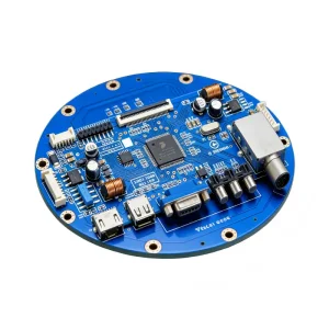
Aluminum-core metal clad substrates (MCPCB) offering high thermal conductivity for industrial lighting.
China LED Module Board PCB Assembly--STHL Manufacturers, Factories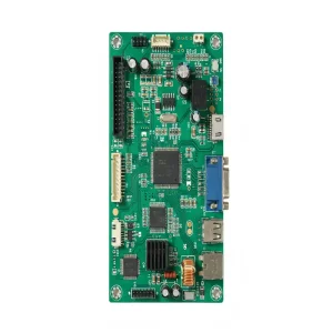
RF shielding, impedance tuning, and high sensitivity for GPS/Galileo navigation modules.
China GPS Receiver PCBA Assembly--STHL Manufacturers, Factory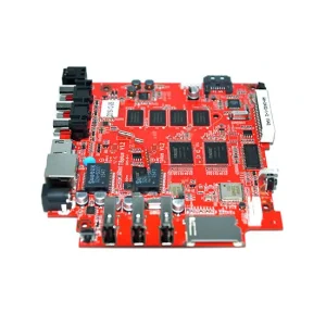
Ultra-low-noise layout architectures engineered for precision directional geophysical instrumentation.
OEM Magnetometer PCBA Assembly--STHL Manufacturers, Factory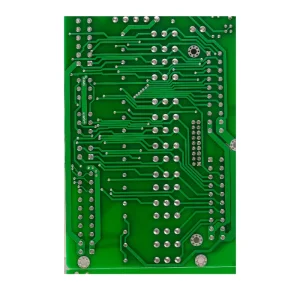
Medical-grade signal isolation boards compliant with ISO 13485 leakage current safety standards.
China ECG Monitor PCB Assembly--STHL Manufacturers, Factory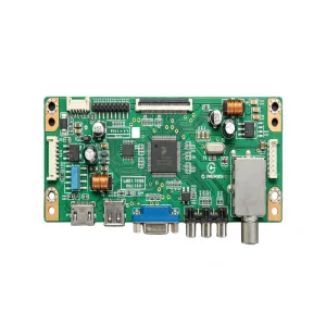
High-sensitivity inductive pulse induction circuitry built for industrial and security screening systems.
OEM Metal Detector PCB Assembly--STHL Manufacturer, Manufacturers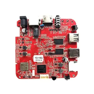
Ultra-low-power standby architectures paired with solar energy harvesting inputs for environmental sensing.
China Ecological Restoration Monitoring Equipment PCB Assembly Manufacturer, Service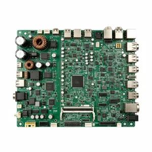
2xMOPP isolation barriers, creepage clearances, and high-efficiency switching converters.
OEM Medical Power Supply PCB Assembly--STHL Manufacturers, Service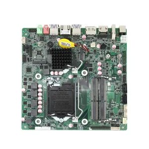
Miniaturized high-density PCBA integration built for multi-parameter clinical testing systems.
High-Quality Biological Monitoring System PCB Assembly--STHL Manufacturer, Manufacturers