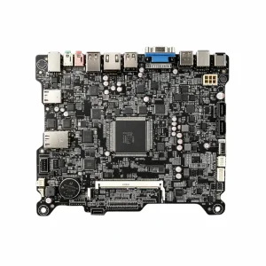
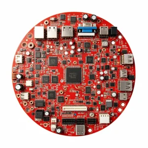
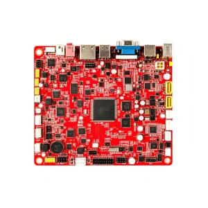
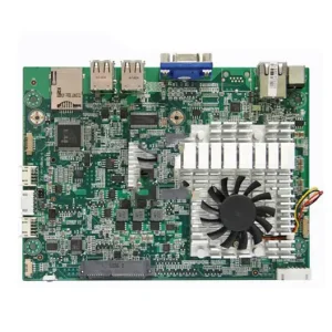
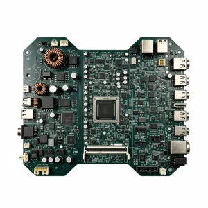
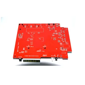
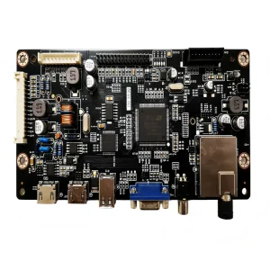
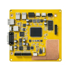
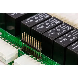
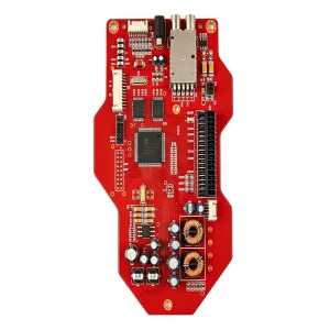
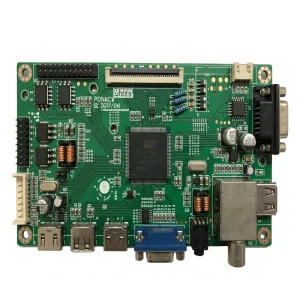
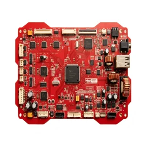
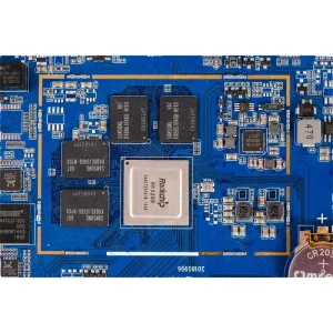
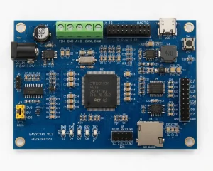
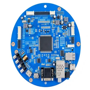
Engineered for instant scalability: Explore our featured OEM power, automotive safety, and IoT hardware assemblies.
Bridging the chasm between rapid hardware iteration, supply chain resilience, and tier-one zero-defect manufacturing standards.
In modern electronic product design, Time-to-Market (TTM) dictates competitive survival. The conventional split model—where hardware engineering teams contract bare-board fabrication, raw-part component brokers, and separate SMT assembly vendors across continents—is no longer viable. Today's global OEMs demand Rapid PCB Assembly (PCBA) ecosystems capable of translating complex multi-layer Gerber topologies and complete Bills of Materials (BOM) into verified physical prototypes and pilot runs within 24 to 72 hours.
Achieving this speed without sacrificing IPC Class 2 or Class 3 reliability standards requires automated Design for Manufacturability (DFM) algorithms, closed-loop Surface Mount Technology (SMT) lines, automated optical/X-ray verification, and institutional traceability across all active and passive electronic components.
Combining the dense supply-chain clusters of the Greater Bay Area with world-class engineering execution.
Situated within the Shenzhen hardware innovation hub, our facility accesses hundreds of authorized component franchisers, silicon distributors, and specialty passives within a 2-hour logistics radius, eliminating international customs holding times for prototypes.
We eliminate friction by integrating bare PCB fabrication, multi-layer stack-up engineering, component procurement, laser stencil manufacturing, SMT mounting, through-hole soldering, and custom enclosure box-build under a single roof.
Western engineering budgets often struggle with prohibitive tooling and non-recurring engineering (NRE) charges. Our flexible tooling and high-speed modular pick-and-place setup provide accessible rapid prototyping without Minimum Order Quantities (MOQ).
Technological imperatives shaping next-generation high-density, automotive, and mission-critical electronics.
Manual engineering review bottlenecks are disappearing. Machine-learning algorithms now parse Gerber layers and centroid data against millions of manufacturing rules, detecting pin-to-pad mismatches and solder bridge liabilities in minutes.
With power densities skyrocketing in high-frequency DC-DC converters and EV chargers, rapid assembly lines must accommodate ultra-thin substrates, copper core boards, and vacuum reflow soldering to dissipate extreme thermal loads without voiding.
Edge AI devices require 0.35mm pitch BGAs, 01005 passives, and blind/buried micro-vias. Rapid SMT manufacturing relies on 3D Solder Paste Inspection (SPI) and Automated X-ray Inspection (AXI) to maintain 100% joint integrity on hidden solder balls.
How rapid turnkey PCBA execution powers mission-critical hardware deployments across global markets.
SRS (Supplemental Restraint Systems) and radar perception modules engineered with zero-delamination substrates, conformal coatings, and IATF 16949-compliant trace tracking.
Ruggedized redundant power supplies and isolated DC-DC converters designed to endure thermal cycling, electrical spikes, and harmonic vibration in demanding 24/7 environments.
ISO 13485-certified PCBA for clinical infusion pumps and body temperature monitors requiring medical-grade signal isolation, biosensing precision, and complete audit-ready records.
High-speed wireless routers, PoE VoIP platforms, and smart energy modules built using controlled impedance topologies, low-loss dielectrics, and automated functional testing.
A strategic framework for hardware supply-chain directors, procurement managers, and systems architects.
Procurement teams require anti-counterfeit protection. Every chip and passive component must be sourced from authorized lines or certified supply-chain partners with manufacturer CoCs and lot-level traceability in ERP/MES records.
Rapid assembly demands proactive component management. Leading EMS facilities analyze BOM health to identify end-of-life (EOL), obsolete, or long-lead items, proposing drop-in pin-compatible alternatives before line stoppage occurs.
Rapid output must not compromise quality. Leading manufacturers combine In-Circuit Testing (ICT), Flying Probe tests for fast turns, 3D AOI/AXI, and dedicated functional jigs (FCT) running proprietary firmware before final packaging.
Addressing core technical questions from sourcing professionals and engineering leads.
For quick-turn prototyping, lead times typically range from 24 to 72 hours following DFM approval and component availability. Turnkey builds that include custom bare-board fabrication and component procurement typically run 5 to 9 working days.
We deploy high-resolution 3D Solder Paste Inspection (SPI) to detect solder volume, height, and area defects prior to component placement. Post-reflow, high-magnification Automated X-Ray Inspection (AXI) checks for solder bridging, voids, and misalignment beneath leadless components.
Yes. We support full turnkey procurement, partial turnkey models, and 100% consigned kit assemblies. In partial turnkey builds, clients provide specialized microcontrollers, sensors, or pre-programmed ASICs, while we source standard passives, connectors, and bare boards.
To deliver an accurate quote and preliminary DFM review within 24 hours, our engineering team requires: (1) Gerber RS-274X or ODB++ files, (2) an Excel BOM complete with Manufacturer Part Numbers (MPN) and footprint references, (3) a Pick-and-Place (Centroid) XY coordinate file, and (4) any specific testing guidelines.
Explore our advanced medical, computing, LED optoelectronic, and uninterruptible power supply assemblies.