Precision-manufactured electronic assemblies optimized via high-speed automated SMD pick-and-place lines, automated optical inspection, and conformal finishing.
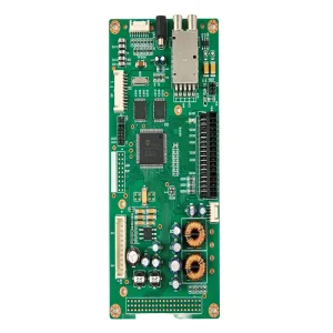
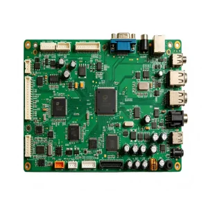
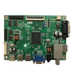
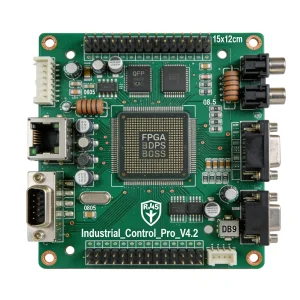
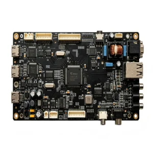

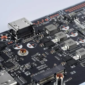
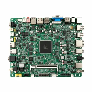
Evaluating the evolution of surface mount electronic manufacturing from rigid component placement to AI-guided, closed-loop cyber-physical assembly systems.
Global industrial demand for ubiquitous computing, wearable biosensors, and millimeter-wave communication has forced printed circuit board assemblies (PCBAs) to accommodate ultra-miniaturized passive components down to 01005 and 03015 form factors. Operating an industrial OEM SMD assembly line requires placement accuracy exceeding ±15 microns at 3-sigma limits.
Traditional mechanical feeder vibrations and pneumatic nozzle fluctuations inevitably cause component skew, tombstoning, and solder bridging. Modern lines integrate multi-spectral vision alignment, linear motor gantry drives, and non-contact vacuum sensing to ensure near-zero defect rates during high-speed cycle runs.
Statistical process analysis across high-volume surface mount production confirms that over 70% of PCBA soldering faults originate directly at the solder paste printing stage. Solder deposit volume inconsistencies, bridging, excessive peaking, and stencil aperture clogging lead to critical field failures.
True Industry 4.0 SMT lines employ closed-loop M2M (Machine-to-Machine) communication between 3D SPI optical scanners and fully automatic stencil printers. Volumetric offset data instantly triggers automatic stencil wipe cycles and alignment micro-adjustments in real-time, eliminating manual calibration latency.
The adoption of RoHS/REACH compliant lead-free alloys (such as SAC305 and low-temperature bismuth-tin formulations) narrows the processing window between alloy melting points (217°C) and FR-4 glass transition temperatures (Tg ≥ 170°C). Non-uniform thermal distribution risks package warpage, Head-in-Pillow (HiP) defects, and intermetallic brittleness.
STHL deploys multi-zone reflow convection ovens utilizing high-purity Nitrogen (< 100 ppm O2) blankets. Inerting prevents copper pad oxidation, improves solder wetting on fine-pitch BGAs (Ball Grid Arrays), and stabilizes intermetallic compound layer (IMC) growth to maximize thermal fatigue resistance.
Why the hyper-converged hardware ecosystem of Shenzhen, China continues to dominate high-mix, low-to-high volume electronics manufacturing services.
While geopolitical diversification has stimulated manufacturing ventures across Southeast Asia and Latin America, high-density surface mount operations remain intrinsically bound to deep physical component supply chains. A missing 0402 ceramic capacitor or passive ferrite bead can halt an entire automated pick-and-place production schedule for weeks in geographically fragmented regions.
Operating within Shenzhen's Bao'an industrial nucleus, STHL commands immediate physical access to over 500,000 active electronic parts through authorized franchise partners (Arrow, Avnet, Digi-Key, Mouser) alongside tier-1 silicon distributors. Custom stencil laser cutting, specialized substrate fab (HDI Any-Layer, ceramic, aluminum, polyimide flex), and customized functional fixture milling are fulfilled within a 4-hour radius.
To combat counterfeit components and silicon obsolescence in international markets, our turnkey procurement protocol enforces strict multi-tier vetting:
From raw Gerber and centroid input to zero-defect box build: A forensic review of our automated cleanroom surface mount manufacturing line.
High-precision automatic printers with closed-loop squeegee pressure control (±0.05 kg/cm). Sub-micron fiducial alignment ensures consistent paste volume deposition across dense 0.3mm pitch QFNs and WLCSP arrays.
Structured light moiré interferometry inspects 100% of printed pads in 3D: measuring height, volume, area, coplanarity, and bridge detection. Real-time feedback alerts upstream printing equipment before defects manifest.
Modular mounters deliver placement speeds up to 100,000+ CPH. Vision inspection heads verify nozzle pick angles, missing leads, and bent pins on the fly, safely placing passive chips down to 01005 and massive 55mm connectors.
Upper and lower independently regulated thermal zones. Closed-loop PID temperature profiling guarantees delta T ≤ ±1.5°C across complex multi-layer boards, terminating with controlled cooling gradients to optimize alloy crystal grain structures.
| SMD Line Engineering Parameter | Standard Technical Capability | High-Precision Advanced Tier | Compliance / Verification Method |
|---|---|---|---|
| Min / Max Board Size | 50 mm × 50 mm / 510 mm × 460 mm | Up to 1200 mm (LED Rigid Light Strips) | Automatic Conveyor Track Width Sensor |
| Min Passive Component Size | 0201 Imperial (0603 Metric) | 01005 & 03015 Micro Metric | Multi-Vision Alignment & Optical Sensors |
| Fine Pitch Component Capabilities | BGA pitch ≥ 0.4 mm, QFP pitch ≥ 0.3 mm | Micro-BGA pitch ≥ 0.25 mm, CSP & PoP | 3D SPI + Automated 3D AOI & AXI |
| Placement Accuracy (μm) | ±25 μm @ 3-sigma | ±15 μm @ 3-sigma | Laser Fiducial Centering Calibration |
| PCB Substrate Technologies | FR-4, High-Tg, Halogen-Free, CEM-3 | Flex, Rigid-Flex, Aluminum, Ceramic, Rogers | IPC-6012 & IPC-6013 Inspection Standard |
| Soldering Atmosphere & Profile | Convection Forced Hot Air | Nitrogen (N2) Tunnel (< 100 ppm O2) | KIC 24/7 Automated Real-Time Profiler |
| Non-Destructive Joint Testing | Post-reflow 2D / 3D Automated Optical (AOI) | High-Resolution 2D/3D X-Ray (AXI) & BGA Ball Void Inspection (<10%) | IPC-A-610 Class 2 & Class 3 Criteria |
Eliminating deployment frictions through comprehensive compliance architectures spanning North America, the European Union, and the Asia-Pacific region.
Automotive electronics cannot tolerate random infant mortality or solder micro-fissures. Our dedicated automotive SMT lines operate strictly under IATF 16949 frameworks, enforcing stringent APQP (Advanced Product Quality Planning), PPAP Level 3 documentation, FMEA defect analysis, and 100% trace serialization.
Medical diagnostic monitors, ventilators, and surgical equipment require rigorous risk management (ISO 14971) and continuous device history record (DHR) tracking. We ensure full adherence to cleanroom air quality, ionic contamination testing, bio-burden controls, and automated conformal coating encapsulation.
Certified in-house IPC trainers oversee all post-reflow and manual soldering personnel. We support standard Class 2 commercial electronics as well as mission-critical Class 3 high-reliability builds where continuous peak performance and zero equipment downtime in harsh operating environments are non-negotiable.
Confidentiality is cemented via legally binding pre-RFQ Non-Disclosure Agreements (NDAs). Design Gerber assets, firmware binaries, and BOM pricing are secured within isolated virtual subnets. Automated on-line IC programming workstations deploy hardware cryptographic tokens to prevent firmware sniffing.
Examine how our integrated SMD assembly facilities power critical hardware across commercial, medical, industrial, and automotive infrastructures.
High-power density automotive assemblies must withstand extreme thermal vibration gradients (-40°C to +125°C). By utilizing heavy copper substrates (>3 oz), selective wave soldering for high-current terminal lugs, and automated polyurethane potting, our PCBA lines achieve zero-defect operational longevity under strict OEM road-safety standards.
Medical diagnostic monitoring demands microvolt-level analog signal integrity alongside high-speed digital processing. Our SMD lines mount ultra-fine pitch sensor interfaces and RF shielding enclosures with zero solder spatter, fully backed by automated cleaning cycles to eradicate flux residues and leakage currents.
Managing multi-cell lithium storage banks requires extreme voltage isolation and rapid balancing response times. STHL integrates thick gold immersion PCB finishes, high-reliability optocouplers, and automated functional burn-in cycling under simulated peak loads to guarantee safety compliance in modern green energy installations.
Forward engineering pathways charting our technological transition toward self-optimizing surface mount assembly environments.
Transitioning beyond standard heuristic pixel comparison algorithms: Deep learning vision models trained on millions of reflow solder joints autonomously classify micro-voids, wettability angles, and lead lift. False call rates drop by 85%, eliminating human inspection fatigue while boosting line throughput.
Deploying comprehensive computational fluid dynamics (CFD) models of our 10-zone reflow tunnels. By simulating board thermal mass, copper layer balance, and component shadows before physical runs, engineers calibrate heating zone parameters digitally, cutting physical prototype iterations to zero.
As silicon scaling encounters thermal and inter-connect limits, System-in-Package (SiP) and embedded passive cavity technologies take center stage. Our future manufacturing pipeline incorporates ultra-thin substrate handling, flip-chip underfill automation, and micro-plasma surface activation for next-gen hardware miniaturization.
Clear, granular insights addressing DFM/DFA parameters, component procurement mechanisms, quality audits, and prototype-to-mass-production lead times.
To deliver an accurate, engineering-verified turnkey quotation within 24 hours, our engineering office requires: 1) Gerber files in RS-274X or ODB++ format including all copper layers, solder mask, silkscreen, and mechanical outline; 2) Bill of Materials (BOM) in Microsoft Excel format detailing exact manufacturer part numbers (MPNs), reference designators, package footprints, and designated second-source alternatives; 3) Centroid / Pick-and-Place file specifying X-Y coordinates, board side (Top/Bottom), and component orientation angles (0–360°); and 4) Clear test guidelines covering In-Circuit Test (ICT), programming procedures, and functional testing parameters.
We operate a zero-tolerance anti-counterfeit protocol compliant with AS5553 and AS6081 aerospace/industrial standards. All electronic components are purchased exclusively via original component manufacturers (OCMs) or direct authorized franchise distributors (Arrow, Avnet, Digi-Key, Mouser, Farnell). When legacy or obsolete components must be acquired via audited open-market brokers, parts undergo comprehensive incoming laboratory validation including high-magnification optical mark inspection, X-ray lead frame analysis, solderability wetting tests, and destructive acid decapsulation die microscopy.
For quick-turn prototyping, when components are on-hand or rapidly procured, our SMT lines can build, inspect, and ship assemblies within 24 to 72 hours. For standard turnkey production contracts (including bare PCB fabrication, turnkey BOM procurement, automated SMD placement, and box build), lead times typically range from 2.5 to 4 weeks depending on specific silicon lead times. We also offer vendor-managed inventory (VMI) and safety-stock warehousing in Shenzhen for scheduled monthly blanket purchase orders.
Every project undergoes a rigorous DFM/DFA review before copper is etched or stencils are cut. Our CAM team checks for: 1) Pad-to-component aspect ratio verification to prevent tombstoning; 2) Solder mask web clearances between fine-pitch IC pins to eliminate solder bridging; 3) Fiducial mark placement stability on both panels and local BGA arrays; 4) Thermal relief balancing on internal ground/power planes to avoid cold solder joints; 5) Panelization routing strategies (V-score vs. mouse-bite tabs) ensuring component clearance during depaneling stress.
Yes. In addition to our 7 automated high-speed SMT lines, our Bao'an facility houses 2 dedicated DIP/THT lines equipped with computerized selective wave soldering and dual-wave nitrogen systems. We regularly build high-complexity mixed boards featuring double-sided SMT reflow, BGA/WLCSP arrays, press-fit industrial backplanes, heavy duty transformers, and custom wire harness integration with complete box build enclosures.
Explore our specialized electronic manufacturing solutions engineered for mission-critical industrial, medical, automotive, and power ecosystems.
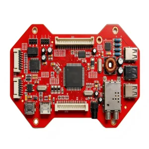


Upload your Gerber files and Bill of Materials (BOM) under a strict Non-Disclosure Agreement. Our Shenzhen engineering team will return a comprehensive Design for Manufacturing (DFM) assessment and production quotation within 24 hours.
