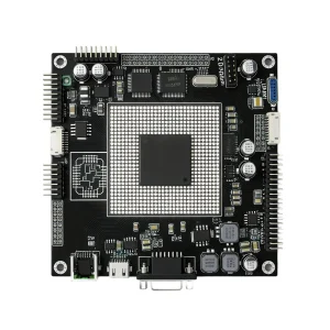
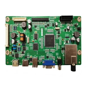
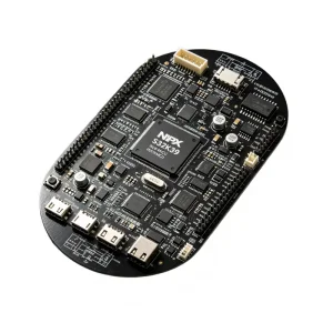
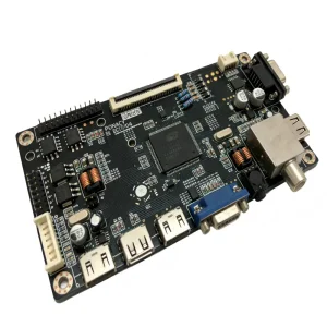
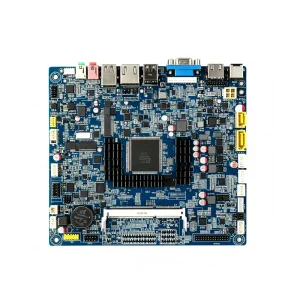
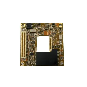
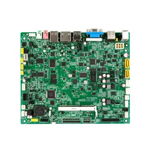
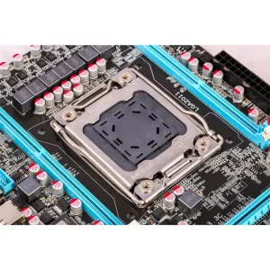
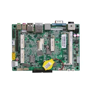
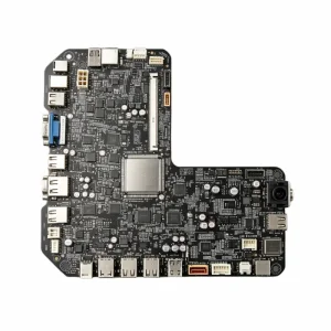
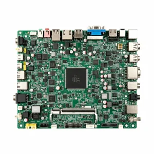
Verified SMT surface mount configurations engineered to IPC-A-610 Class 2 & Class 3 standards, deployed across automotive, healthcare, and high-frequency infrastructure.
Surface Mount Device (SMD) and Surface Mount Technology (SMT) assembly operations require multi-phase precision calibration. Modern electronics cannot tolerate placement deviations, insufficient wetting, or unmitigated solder voiding.
Fully automated screen printers utilize laser-cut, electro-polished nickel stencils. Solder paste height, volume, and bridge integrity are verified in-line via 3D SPI (Solder Paste Inspection) systems before component placement.
Modular pick-and-place systems mount complex passive components (down to 01005 footprints) and active ultra-fine pitch BGAs, CSPs, and QFNs with placement repeatability tolerances within ±0.03mm.
Multi-zone nitrogen-purged reflow ovens stabilize thermal profiles. Precise control across preheat, soak, reflow, and cooling stages limits thermal stress while minimizing solder voiding rates below 10%.
Every PCBA undergoes 3D Automated Optical Inspection (AOI) to detect misalignments, tombstones, and solder bridges. Critical BGA and hidden-pad junctions pass through non-destructive 3D Automated X-ray Inspection (AXI).
| SMD Engineering Parameter | Standard OEM Specification | Advanced / High-Reliability Capability | Quality Verification Baseline |
|---|---|---|---|
| Min. Passive Footprint | 0201 metric (0.6mm × 0.3mm) | 01005 / 03015 ultra-miniature passives | In-line 3D AOI + High-Res Optical Microscopy |
| Fine-Pitch IC & Ball Pitch | 0.40mm BGA / 0.35mm QFP Lead Pitch | 0.30mm Micro-BGA, Wafer-Level CSP | High-Resolution 3D X-Ray Inspection (AXI) |
| Solder Paste Profiling | SAC305 Lead-Free (RoHS) | High-Reliability Indium / Low-Void Ag-Alloy | 3D SPI Volumetric Tolerance <10% |
| Substrate Compatibility | FR-4 Multi-layer (4–16 Layers) | Rigid-Flex, HDI Any-Layer, Metal-Core (IMS), Rogers RF | IPC-6012 & IPC-6013 Microsectioning Audits |
| Reflow Atmosphere | Air Atmosphere Convection | Closed-Loop Nitrogen (N2) <500ppm O2 Residual | Thermal Datalogger Profiling on Golden Boards |
Shenzhen represents the epicentre of global electronic manufacturing. Contract manufacturing here provides speed, cost elasticity, component availability, and engineering scalability that fragmented regional plants cannot match.
Within a 50-kilometer radius in Bao'an, Shenzhen, engineers can secure raw bare copper boards, specialty passives, silicon wafers, custom heat sinks, injection tooling, and CNC enclosures within 24 hours.
Direct supply partnerships with over 100 franchised global distributors (Digi-Key, Mouser, Arrow, Avnet, Microchip, STMicroelectronics) prevent grey-market incursions and eliminate counterfeit part risks.
Our 7 automated SMT lines provide elastic scheduling. Prototype runs migrate into multi-million-unit mass production without changing line configurations, tooling setups, or QA oversight teams.
Overseas procurement demands absolute transparency, legal non-disclosure protection, strict intellectual property defense, and adherence to environmental directives.
Gerber matrices, firmware binaries, and proprietary schematics are secured behind encrypted access nodes. Formal non-disclosure agreements precede any engineering document review.
Every PCB is laser-etched with a unique 2D Matrix Data code linking each component back to feeder positions, operator ID, solder paste batch, and reflow profile archives.
Manufacturing lines run lead-free (RoHS compliant), non-halogenated fluxes, and full REACH-compliant materials, ensuring finished assemblies can enter EU and North American markets smoothly.
Fluent English-speaking hardware engineering teams conduct comprehensive Design for Manufacturability (DFM) and Design for Testing (DFT) reviews prior to stencil release.
Enterprise procurement requirements have shifted from low-cost sourcing toward end-to-end supply stability, high-frequency performance, and integrated IoT architectures.
As wearable medical diagnostics, AR peripherals, and smart locks demand reduced footprints, SMT lines must support 01005 passives alongside flip-chip and die-attach processes.
Key Focus: Void reduction below 8% in thermal pad geometries.
High-voltage automotive onboard chargers (OBC) and industrial inverters are migrating to Gallium Nitride (GaN) and Silicon Carbide (SiC) switches with strict thermal dissipation requirements.
Key Focus: Heavy copper assembly and vacuum vapor-phase soldering.
High-frequency communication hardware requires controlled impedance bare boards, low-loss dielectric laminates, and RF shielding cages positioned with sub-millimeter accuracy.
Key Focus: Automated conformal coating and selective potting.
Our SMT process lines are engineered to meet the operational demands of diverse field environments, from industrial conditions to high-reliability medical devices.
Under-the-hood engine compartments and chassis electronics require IATF 16949-audited processes that withstand continuous vibration, thermal cycling, and moisture exposure.
Manufactured in strict compliance with ISO 13485 standards, featuring lot-level traceability, automated pin-level optical inspection, and functional verification across every batch.
Heavy duty electronics deployed in outdoor infrastructure, continuous 24/7 operating regimes, and power sub-stations requiring high surge tolerance and weatherproofing.
Comprehensive engineering and commercial insights to help overseas hardware managers, supply chain leads, and sourcing engineers qualify our manufacturing lines.
Advanced SMT surface mount configurations engineered to IPC-A-610 Class 2 & Class 3 standards, deployed across automotive, healthcare, and high-frequency infrastructure.